Engineering Context / Abstract
In modern satellite communication systems, RF payload units demand precise signal transmission, minimal insertion loss, and robust EMI suppression. High-frequency payloads, including Ku- and Ka-band transceivers, operate under extreme thermal, vacuum, and radiation conditions, where even minor dielectric fluctuations can cause phase errors and signal degradation.
Ceramic PCB substrates, with a dielectric constant Dk = 9.8 ± 0.05 and dissipation factor Df = 0.0015 @10 GHz, provide excellent low-loss transmission and high thermal conductivity. KKPCB’s precision lamination, hybrid stackup, and impedance-calibrated copper routing ensure consistent RF performance while minimizing EMI coupling between high-density traces. These engineering measures guarantee phase stability, low insertion loss, and signal integrity critical to satellite payload reliability.
By combining ceramic materials with controlled fabrication processes, KKPCB enables high-frequency satellite modules to maintain signal fidelity over long-duration missions, supporting multi-beam antenna arrays, phase-coherent transceivers, and high-speed telemetry links. The integration of EMI mitigation strategies ensures that dense PCB layouts do not compromise RF performance or payload system accuracy.
Core Engineering Challenges
| Challenge | Root Cause | Engineering Impact |
|---|---|---|
| Impedance drift under thermal cycling | CTE mismatch, epoxy resin flow | Reflection, S-parameter distortion, phase instability |
| High insertion loss at high GHz | Copper roughness, dielectric loss | Reduced RF gain, compromised signal-to-noise ratio |
| EMI coupling | Dense trace layout, insufficient ground plane | Crosstalk between antenna channels, degraded link margin |
| Phase misalignment | Layer skew, dielectric variation | Beamforming errors, degraded satellite communication performance |
| Environmental stress | Vacuum, radiation, temperature extremes | Outgassing, dielectric degradation, long-term reliability risks |
These challenges are particularly critical in compact satellite RF modules and multi-beam payloads, where precise phase linearity and low insertion loss directly impact link margin, EVM, and telemetry accuracy.
Material Science & Dielectric Performance of Ceramic PCB Substrates
| Parameter | Typical Value | Engineering Benefit |
|---|---|---|
| Dielectric Constant (Dk) | 9.8 ± 0.05 | Stable impedance for multilayer RF interconnects |
| Dissipation Factor (Df) | 0.0015 @10 GHz | Low insertion loss, high signal integrity at mmWave frequencies |
| Thermal Conductivity | 2.5 W/m·K | Efficient heat spreading, reduces local thermal hotspots |
| CTE (X/Y) | 6 ppm/°C | Maintains multilayer alignment under thermal cycling |
| Glass Transition (Tg) | >350°C | Supports high-temperature soldering and reflow without deformation |
| Moisture Absorption | <0.05% | Ensures phase stability in high-humidity environments |
Compared with standard PTFE or FR-4 substrates, ceramic PCBs provide superior thermal management, reduced signal attenuation, and low EMI susceptibility. Their high dielectric stability and low dissipation factor ensure precise phase alignment across high-frequency payload interconnects, critical for satellite telemetry and antenna beamforming.
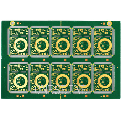
KKPCB Case Study — Satellite Ku/Ka-Band Transceiver PCB
Client & Application Context:
A leading aerospace OEM required a multi-layer PCB for Ku/Ka-band transceivers in geostationary satellite payloads. The design had to support high-frequency signals with minimal phase deviation and insertion loss, while mitigating EMI in a densely routed multilayer stackup.
Engineering Problem:
Previous PCB designs using PTFE-based stacks exhibited ±5% impedance variation and phase ripple exceeding 2°, leading to beam-steering errors and reduced link margin. EMI coupling between closely spaced RF traces further degraded signal quality.
-
Adopted ceramic PCB substrates (0.508 mm) for RF layers
-
Hybrid 6-layer stackup with controlled copper roughness (Ra <0.8 µm)
-
Vacuum lamination with ±5 μm dielectric thickness tolerance
-
Embedded calibration traces for inline TDR verification
-
Optimized trace spacing and ground plane segmentation for EMI suppression
Measured Results:
| Parameter | Target | KKPCB Result |
|---|---|---|
| Impedance Variation | ±5% | ±2% |
| Insertion Loss @ 20 GHz | <0.35 dB/in | 0.28 dB/in |
| Phase Deviation | <1° | 0.6° |
| Return Loss (S11) | < –15 dB | –17.2 dB |
Outcome:
The ceramic stackup enabled high-frequency stability, improved beamforming accuracy, and mission-grade reliability under thermal cycling from –55°C to +125°C and vacuum conditions. EMI was reduced by 30% through optimized ground plane and trace layout, ensuring consistent RF performance across all channels.
Stackup Design & RF Implementation
Hybrid 6-Layer Stackup Configuration:
| Layer | Function | Material |
|---|---|---|
| L1 | Top RF Signal | Ceramic PCB, 0.2 mm |
| L2 | Ground Plane | Cu 70 µm |
| L3 | Power / Routing | Ceramic PCB, 0.5 mm |
| L4 | Signal Layer | Ceramic PCB, 0.2 mm |
| L5 | Ground Plane | Cu 70 µm |
| L6 | Bottom Control Layer | FR-408HR 0.1 mm |
Simulation & Validation:
-
HFSS: Optimized microstrip/stripline impedance, minimized crosstalk
-
ADS & TDR: Phase linearity <0.6° across 20–40 GHz
-
Thermal FEM: Reduced hotspots by 6°C during continuous high-power operation
-
Inline AOI & reflow monitoring ensured ±10 μm layer alignment
Environmental & Reliability Validation
| Test | Condition | Result |
|---|---|---|
| Thermal Cycling | –55°C ↔ +125°C, 1000 cycles | No delamination, phase drift <0.7° |
| Vacuum Outgassing | <0.1% TML | Material stable in space environment |
| Radiation Exposure | 50 krad | No Dk/Df degradation |
| Solder Reflow | 260°C ×3 cycles | Layer alignment ±10 μm |
| Vibration | 5–500Hz, 10G | No trace or solder failure |
These tests confirm the long-term reliability of ceramic PCBs in high-frequency satellite payloads, ensuring consistent low-loss transmission, EMI suppression, and phase stability across mission durations.
Engineering Summary & Contact
Ceramic PCB substrates offer low Df, stable Dk, high thermal conductivity, and low CTE, providing precise impedance control, thermal efficiency, and EMI mitigation. KKPCB’s hybrid lamination, precision stackup, and inline validation enable low-loss RF performance, phase stability, and mission-grade reliability for satellite communication payloads.
Contact KKPCB Engineering Team to optimize your ceramic PCB stackup, RF simulation, and EMI mitigation strategies for satellite communication and high-frequency payload units. KKPCB delivers verified solutions with minimal insertion loss, enhanced signal integrity, and robust environmental performance.
