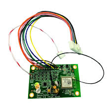
Zigbee Module PCB: The Core of Building Reliable, Low-Power IoT Networks

In the rapidly expanding Internet of Things ecosystem, choosing the right wireless technology determines both system performance and long-term scalability. Among various communication standards, the Zigbee Module PCB stands out as the backbone for low-power, large-scale mesh networks used in smart homes, industrial automation, smart agriculture, and building management systems.
This article provides an in-depth technical exploration from an IoT architect’s perspective, focusing on protocol stack insights, RF engineering, power optimization, network topology, system integration, and security—the essential factors behind a successful Zigbee device design.
1. Deep Dive into the Zigbee Protocol Stack

Zigbee is built on the IEEE 802.15.4 standard and optimized for low-rate, low-power wireless personal area networks (LR-WPANs), making it ideal for scenarios requiring huge node counts, self-healing, and low energy consumption.
Key Layers Overview
Physical Layer (PHY)
-
Works primarily in the 2.4 GHz ISM band
-
Regional Sub-GHz options: 868 MHz (EU), 915 MHz (US)
-
Sub-GHz Zigbee Modules provide stronger penetration & longer range.
MAC Layer
Manages channel access, acknowledgments, and reliable frame delivery, even in congested RF environments.
Network Layer (NWK)
The heart of Zigbee:
-
Enables route discovery, route repair, and mesh formation
-
Ensures automatic rerouting when a node fails (true self-healing)
Application Layer (APL)
Provides:
-
APS (Application Support Sublayer)
-
ZDO (Zigbee Device Object)
-
Manufacturer-defined application objects
Enabling multi-vendor interoperability.
2. How Zigbee Compares with Other Wireless Technologies
| Feature | Zigbee Module PCB | Bluetooth Mesh PCB | WiFi 6 Module PCB | NB-IoT Module PCB |
|---|---|---|---|---|
| Topology | Full Mesh | Broadcast Mesh | AP-STA | Cellular Star |
| Data Rate | 250 kbps | ~1 Mbps | Up to 9.6 Gbps | ~127 kbps |
| Power Consumption | Ultra-Low | Low | High | Ultra-Low |
| Node Capacity | >65,000 | >32,000 | Hundreds | >50,000 |
| Typical Use | Smart Home, Industrial Control | Lighting, Tracking | High-speed data | Smart meters |
Zigbee finds the ideal balance between power consumption, network scale, and self-healing mesh capabilities.
3. Critical RF & Antenna Design Techniques for Zigbee PCBs
RF engineering is the decisive factor for communication reliability. Poor layout can reduce transmission range, increase packet loss, and drain battery life.
Antenna Options
-
PCB Antennas (IFA / Meandered IFA)
-
Lowest cost
-
Requires precise tuning & antenna clearance
-
-
Chip Antennas
-
Stable performance
-
Easy to integrate following manufacturer guidelines
-
-
External Antennas (IPEX / SMA)
-
Best range & flexibility
-
Ideal for industrial and long-range use-cases
-
RF Design Rules
-
Maintain a 50-ohm RF path from chip to antenna
-
Keep RF traces short, straight, and isolated
-
Provide a clean, continuous ground plane
-
Avoid routing under antenna or RF lines
-
Use π-matching circuits for final tuning
-
Add high-quality decoupling capacitors near RF power pins
4. Zigbee Network Topology and Device Roles
Device Roles
-
Coordinator – creates the network, manages addresses & keys
-
Router – forwards data, expands coverage
-
End Device – ultra-low-power sleep mode sensor/actuator
Topologies
-
Star – simple, limited coverage
-
Tree – extended range but fixed paths
-
Mesh – best robustness (multiple paths, self-healing)
Large-scale Zigbee systems (smart buildings, factories) typically rely on dense router placement and multi-layer PCB designs for improved signal integrity.
5. Extreme Power Optimization for Long Device Lifespan
Zigbee end devices often operate on coin-cell batteries for years.
Key Power-Saving Strategies
-
Select ultra-low quiescent current regulators & sensors
-
Choose DCDC for efficiency or LDO for low noise
-
Use load switches for peripherals
-
Maximize deep sleep time
-
Utilize Zigbee’s polling & buffering mechanisms
Typical Power Consumption
Mode |
Current |
|---|---|
| Deep Sleep | 1–3 µA |
| Processing | 3–5 mA |
| RX | 15–20 mA |
| TX | 25–35 mA |
When optimized, a Zigbee end-device can achieve 10–12 years of battery life.
6. System Integration, Gateway Role & Edge Computing
Zigbee Gateway
Often integrates:
-
Zigbee Module PCB (local mesh communication)
-
WiFi 6 / Ethernet / LTE Module PCB (cloud backhaul)
Edge Computing
-
Local decision-making reduces latency
-
Preprocessing reduces cloud bandwidth & cost
-
Enhances reliability during network outages
7. Security & Deployment Best Practices
Zigbee embeds robust security mechanisms:
-
AES-128 encryption
-
Network Key + Link Key protection
-
Secure joining procedures
Large-scale deployment checklist
-
Conduct site RF survey
-
Plan router positions & channel allocation
-
Use automated provisioning scripts
-
Enable OTA firmware updates
-
Monitor network health & battery levels via cloud
Conclusion
The Zigbee Module PCB is far more than a simple wireless board—it is the strategic foundation of low-power, scalable IoT system design.
Mastering antenna engineering, RF layout, power optimization, mesh topology, gateway integration, and system security determines whether an IoT project can operate reliably for years.
With careful design and high-precision PCB/PCBA manufacturing, a Zigbee module becomes the bridge connecting real-world sensing to intelligent digital infrastructure.

