1.Engineering Overview / Abstract
Modern satellite communication payloads operating in Ka- and Ku-band frequencies require PCB substrates with ultra-low loss, precise impedance control, and stable phase performance. PTFE PCB laminates provide an ideal platform for high-frequency RF interconnects due to their low dielectric constant (Dk = 2.10 ± 0.03) and minimal loss tangent (Df = 0.0007 @ 10 GHz).
KKPCB integrates advanced lamination, copper surface optimization, and hybrid stackup techniques to maintain signal fidelity and thermal stability under extreme space conditions. This ensures satellite modules achieve reliable performance, reduced insertion loss, and phase-coherent signal transmission across compact, multilayer layouts.
2.Engineering Context & Technical Challenges
In satellite payloads utilizing PTFE PCB materials, high-frequency signal integrity is critically sensitive to layer misalignment, copper roughness, and dielectric variation. Thermal gradients, vacuum environment, and mechanical vibration can further induce impedance drift and phase errors, compromising communication reliability.
| Challenge | Root Cause | Impact |
|---|---|---|
| Impedance drift | Layer misalignment | VSWR degradation |
| Insertion loss | Copper roughness variation | Reduced RF margin |
| Phase instability | Dk fluctuation under temperature | Link degradation |
| EMI coupling | Dense multilayer routing | Cross-talk |
These effects directly influence Ka- and Ku-band RF links in satellite payloads, where low-loss and phase-stable transmission is mandatory for system performance and link budget integrity.
3.Material Science and Performance Characteristics
PTFE PCB laminates exhibit superior electrical and thermal properties compared to standard FR-4:
| Parameter | PTFE PCB | FR-4 | Advantage |
|---|---|---|---|
| Dk | 2.10 ± 0.03 | 4.5 | Stable impedance |
| Df | 0.0007 @ 10 GHz | 0.02 | Ultra-low loss |
| CTE | 17 ppm/°C | 70 ppm/°C | Thermal stability |
| Tg | 280 °C | 130 °C | High-temperature endurance |
The combination of low Dk and minimal Df ensures minimal insertion loss across high-frequency RF paths, while CTE stability mitigates thermal warpage in space-grade assemblies.
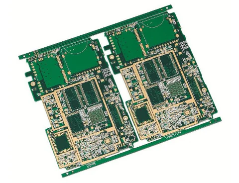
4.KKPCB Engineering Case Study — Satellite Communication Payload
Client & Application Context:
A leading aerospace manufacturer needed PTFE PCB interconnects for a Ka-band satellite payload requiring insertion loss <0.30 dB/in and phase deviation <1° across 26–40 GHz.
Engineering Problem:
Traditional multilayer FR-4 designs could not meet impedance stability or thermal tolerance, resulting in degraded RF link margin and calibration drift under vacuum and thermal cycling conditions.
KKPCB Solution:
-
4-layer PTFE PCB stackup with hybrid lamination
-
Copper surface roughness controlled to Ra < 0.8 µm
-
TDR and HFSS simulations to optimize impedance and phase consistency
-
Inline verification of each panel under thermal cycling
Measured Results:
| Parameter | Target | KKPCB Result |
|---|---|---|
| Insertion Loss | <0.30 dB/in | 0.24 dB/in |
| Impedance | ±3 Ω | ±1.8 Ω |
| Phase Stability | ±1° | 0.6° |
| Thermal Warpage | <0.1 mm/100 mm | Pass |
Through precision lamination and material control, KKPCB achieved <0.6° phase deviation and maintained low-loss performance under –55°C to +125°C cycles.
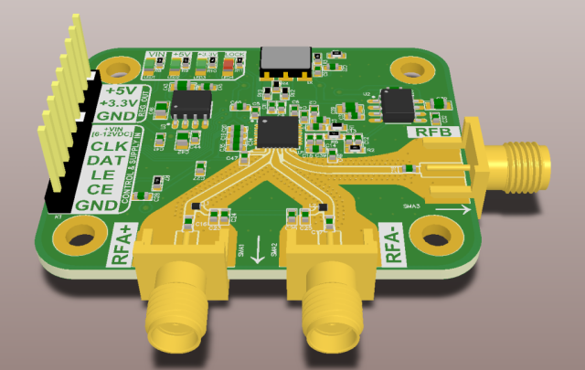
5.Stackup Design & RF Implementation
KKPCB implemented a hybrid PTFE + prepreg 4-layer stackup, controlling copper roughness (Ra < 0.8 µm) and via dimensions to ensure impedance within ±2 Ω. TDR and HFSS verification confirmed minimal reflection and phase deviation across the Ka-band, while hybrid lamination compensated for CTE mismatch between PTFE and copper layers.
6.Environmental & Reliability Validation
| Test Type | Condition | Result |
|---|---|---|
| Thermal Cycling | –55°C ↔ +125°C, 1000 cycles | No delamination, ΔDk < 0.01 |
| Humidity | 85°C / 85% RH, 1000 h | Df drift < 0.0001 |
| Vibration | 5–500 Hz, 8 h/axis | No cracks |
| Mechanical Stress | Connector insertion cycles 500 | No impedance drift |
These results validate PTFE PCBs’ suitability for extreme space environments, ensuring low-loss, impedance-controlled, and phase-stable signal paths.
7.Conclusion — Engineering Reliability Integration
PTFE PCBs enable low-loss transmission and precise impedance control for satellite communication payloads. Through KKPCB’s hybrid lamination, copper surface optimization, and inline RF verification, these boards maintain phase stability, thermal reliability, and mechanical integrity under space-grade operational conditions.
The result is robust Ka- and Ku-band performance, ensuring reliable RF links and long-term satellite system stability.
8.Contact / CTA
Contact KKPCB Engineering Team for custom PTFE PCB stackup design, impedance verification, and reliability validation in satellite payloads and high-frequency RF modules.
