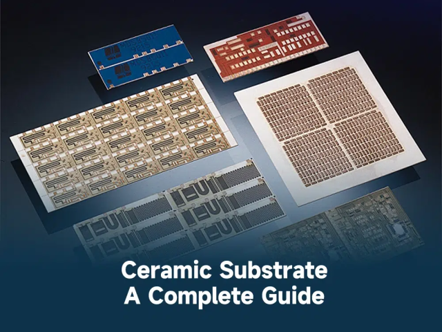
1. Engineering Overview
As laptop and server architectures evolve toward higher clock rates and denser power delivery networks, PCB substrates must withstand increasing thermal stress and EMI coupling.
Ceramic PCB materials, with their excellent dielectric stability and superior thermal conductivity (>20 W/m·K), provide a robust platform for managing power transients and high-frequency switching noise in multi-GHz domains.
KKPCB’s RF process integration ensures that the theoretical advantages of ceramic materials translate into stable, production-grade performance for enterprise and computing systems.
2. Engineering Context & Technical Challenges
In high-performance laptop and server motherboard designs, switching converters and processor power rails generate rapid current transients. These induce EMI coupling across adjacent layers, leading to noise injection, phase distortion, and temperature gradients.
Typical challenges in Ceramic PCB-based systems include:
-
Managing heat dissipation from multi-core processors (>120 W TDP)
-
Controlling impedance for GHz-range signal traces
-
Maintaining dielectric uniformity across power and RF planes
-
Reducing EMI propagation between high-speed digital and RF domains
Without precise control of these parameters, signal integrity and system reliability degrade, particularly in high-density BGA and VRM regions.
3. Material Science and Performance Characteristics
Ceramic PCB substrates used in KKPCB’s process platform feature:
-
Dielectric Constant (Dk): 9.8 ± 0.3 @ 10 GHz
-
Dissipation Factor (Df): 0.0001 @ 10 GHz
-
Thermal Conductivity: > 22 W/m·K
-
CTE (Coefficient of Thermal Expansion): 6.0 ppm/°C
Compared to PTFE or BT Epoxy laminates, Ceramic PCBs exhibit 70–80% lower thermal resistance and 10x higher heat dissipation, ensuring more uniform temperature gradients and reduced hot spots during sustained power loads.
4. KKPCB Engineering Case Study
Client & Application:
A leading Asian server OEM sought to improve VRM thermal control and EMI suppression using a Ceramic PCB-based power distribution board.
Engineering Problem:
Excessive heat buildup near processor power stages caused EMI drift and power instability during 48-hour endurance testing.
-
Integrated Ceramic dielectric substrate with embedded copper-in-ceramic vias for efficient heat spreading.
-
Applied vacuum lamination and surface polishing to reduce conductor roughness (Ra < 0.6 µm).
-
Implemented EMI shielding stackup with internal reference planes.
Results:
| Parameter | Target | KKPCB Result |
|---|---|---|
| Thermal Resistance | < 1.2 °C/W | 0.85 °C/W |
| EMI Attenuation | > 25 dB @ 10 GHz | 28 dB |
| Power Efficiency | > 92% | 93.4% |
| Phase Stability | < 1° | 0.8° |
The optimized Ceramic PCB substrate enhanced current-handling capacity while maintaining EMI suppression and signal linearity under heavy computational load.
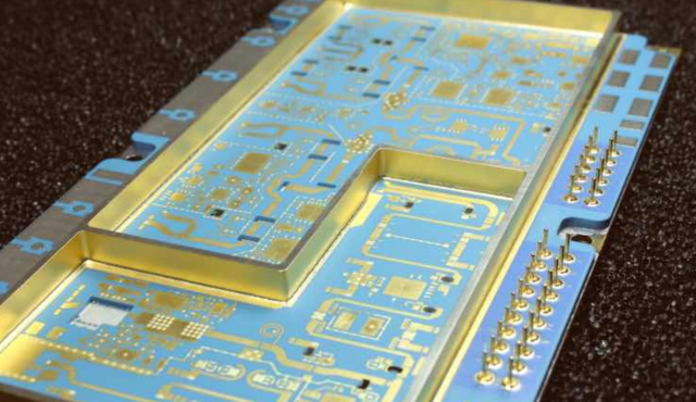
5. Stackup Design & RF Implementation
KKPCB’s hybrid stackup incorporated a ceramic dielectric layer between copper foils and a thin FR-4 reinforcement for mechanical support.
Key features:
-
Embedded ground shielding between power and RF planes
-
4-layer RF + power integration design
-
Controlled impedance within ±3% verified through TDR scanning
-
Cross-validated via HFSS simulations up to 30 GHz
This configuration improved phase alignment and minimized loop inductance in high-speed processor zones.
6. Environmental & Reliability Validation
| Test Type | Condition | Result |
|---|---|---|
| Thermal Cycling | –55°C ↔ +150°C, 1000 cycles | No delamination, <0.15° phase drift |
| Power Endurance | 96 hours @ full load | Stable EMI suppression |
| Humidity Exposure | 85°C / 85% RH, 1000 h | Df variation < 0.0002 |
| Mechanical Shock | 10 G, 6 axes | No crack or impedance drift |
These results confirm the Ceramic PCB’s robustness for long-term laptop and server operation where continuous heat and current stress are present.
7. Conclusion — Engineering Reliability Integration
The Ceramic PCB demonstrates outstanding power integrity, thermal management, and EMI suppression for high-performance computing modules.
Through KKPCB’s hybrid lamination and RF process control, these boards deliver superior reliability, reduced signal noise, and consistent impedance profiles across extreme thermal and electrical conditions.
8. Contact
Contact KKPCB Engineering Team for customized Ceramic PCB stackup design, impedance verification, and reliability testing across server, laptop, radar, and RF communication systems.
