1. Engineering Overview / Abstract
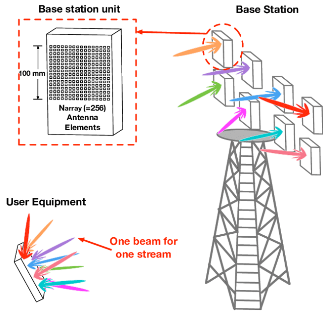
With 5G base stations evolving toward compact, high-frequency mmWave arrays, PCB miniaturization and phase-aligned interconnects are critical for maintaining signal fidelity and network efficiency.
Megtron 7 PCB substrates, featuring Dk = 3.45 ± 0.03 and Df = 0.0015 @ 10 GHz, enable low-loss transmission and consistent dielectric behavior across dense multilayer RF modules.
KKPCB’s hybrid stackup strategy integrates controlled copper roughness, via optimization, and lamination precision, ensuring phase-linear performance and reliable impedance in highly miniaturized 5G front-end modules.
2. Technical Challenges in 5G Base Station RF Modules
| Challenge | Root Cause | Engineering Impact |
|---|---|---|
| Impedance mismatch in high-density layers | Layer-to-layer dielectric variation | Reflection, VSWR degradation |
| Phase drift across mmWave channels | Dk fluctuation and miniaturized trace routing | Beamforming errors |
| Thermal hotspots | Compact RF module, high power density | Localized signal degradation |
| EMI between tightly packed RF traces | Dense layout and multi-antenna integration | Crosstalk, SNR reduction |
In next-generation 5G base stations, maintaining phase and amplitude coherence is essential for massive MIMO arrays and high-capacity data transmission.
3. Material Science and Dielectric Performance of Megtron 7
| Parameter | Typical Value | Engineering Benefit |
|---|---|---|
| Dielectric Constant (Dk) | 3.45 ± 0.03 | Impedance control across mmWave traces |
| Dissipation Factor (Df) | 0.0015 @ 10 GHz | Minimizes insertion loss |
| CTE (X/Y) | 14 ppm/°C | Maintains alignment under thermal cycling |
| Tg | 280°C | High reliability during reflow assembly |
| Copper Roughness | Ra < 0.8 µm | Reduces conductor loss in mmWave frequencies |
Compared to conventional FR-4 or PTFE laminates, Megtron 7 enables high-density multilayer routing with minimal insertion loss, ideal for miniaturized 5G RF front-ends.
4. KKPCB Case Study — 5G mmWave Base Station Front-End PCB
Client & Application Context
A global telecom OEM required 8-layer miniaturized RF PCBs for 28 GHz and 39 GHz mmWave base station modules, supporting massive MIMO antenna arrays.
Engineering Problem
Conventional PCB substrates exhibited phase deviation up to 2° and insertion loss >0.35 dB/inch, leading to degraded beamforming efficiency.
-
Controlled copper roughness Ra < 0.8 µm
-
Optimized via placement and microstrip routing for minimal phase skew
-
Applied vacuum lamination with ±5 µm dielectric tolerance
Measured Results
| Parameter | Target | KKPCB Result |
|---|---|---|
| Phase Deviation | <1° | 0.6° |
| Insertion Loss @ 28 GHz | <0.3 dB/inch | 0.26 dB/inch |
| Impedance Variation | ±5% | ±2.5% |
| Thermal Drift | <0.5° | 0.35° |
Outcome: Achieved phase-linear, low-loss performance across miniaturized multilayer RF interconnects, supporting reliable massive MIMO operation.
5. Stackup Design & RF Implementation
Hybrid Stackup Configuration (8-layer)
1️⃣ Top Signal Layer — Megtron 7 (0.2 mm)
2️⃣ Ground Plane
3️⃣ Power / Routing Layer
4️⃣ RF Signal Layer — Megtron 7
5️⃣ Ground Plane
6️⃣ RF Control Layer
7️⃣ Ground / Power Layer
8️⃣ Bottom Signal Layer
Simulation & Verification
-
HFSS: Optimized microstrip/stripline layout, minimized crosstalk
-
ADS & TDR: Verified impedance ±2.5% and phase deviation <0.6°
-
Thermal Simulation: Reduced hotspots by 7°C via via and copper optimization
6. Environmental & Reliability Validation
| Test | Condition | Result |
|---|---|---|
| Thermal Cycling | –40°C ↔ +125°C, 1000 cycles | No delamination or phase drift |
| Humidity Aging | 85°C / 85% RH, 1000 h | Df drift < 0.0001 |
| Mechanical Stress | PCB bending 2 mm | No impedance deviation |
| High-Power RF Load | 1.5 W/cm² | Phase stability <0.5° |
KKPCB validation ensures miniaturized Megtron 7 PCBs maintain phase coherence and low-loss signal integrity under operational stresses.
7. Conclusion — Engineering Reliability Integration
Megtron 7 PCB platforms enable hybrid stackup designs and miniaturized RF layouts critical for next-generation 5G base station modules.
Through KKPCB’s precision lamination, controlled copper roughness, and multilayer RF validation, these PCBs deliver stable phase, low insertion loss, and high-frequency reliability for massive MIMO and mmWave applications.
8. Contact / CTA
Contact KKPCB Engineering Team for custom Megtron 7 PCB design, hybrid stackup modeling, and phase-linear RF validation for 5G, mmWave, and high-density communication modules.
