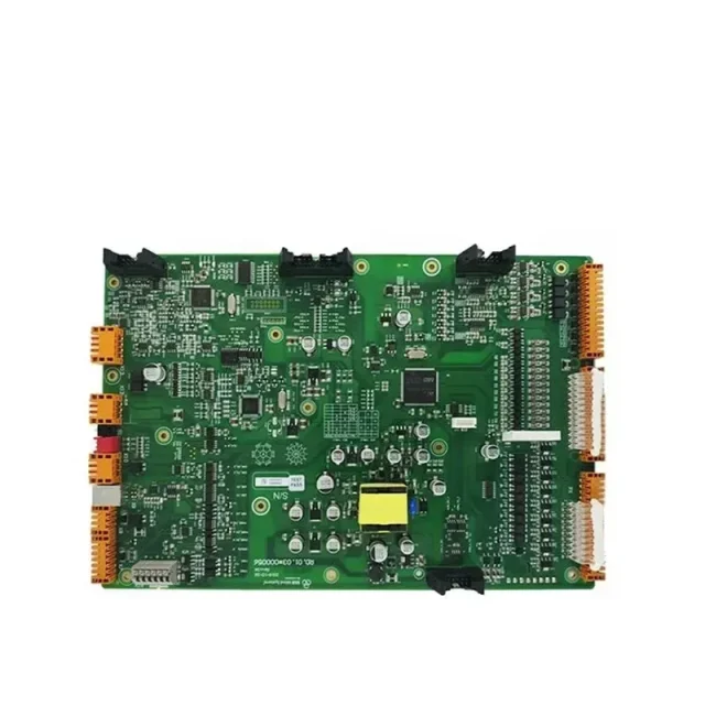
As 5G technology drives faster data rates, lower latency, and higher bandwidth, the complexity of 5G modules continues to increase. A 5G module integrates RF front-end circuits, baseband processing, power management, and high-speed interfaces into a compact design. 5G module PCB assembly plays a critical role in ensuring stable RF performance, signal integrity, and long-term reliability.
Due to high operating frequencies and dense layouts, 5G module PCB assembly requires advanced manufacturing processes and strict quality control.
What Is 5G Module PCB Assembly?
5G module PCB assembly refers to the assembly of printed circuit boards used in 5G communication modules, including:
-
RF front-end modules
-
5G modem and transceiver modules
-
mmWave and Sub-6 GHz modules
-
Integrated antenna and communication modules
These PCBs often combine high-frequency RF circuits with high-speed digital signals, making assembly precision essential.
Key Challenges in 5G Module PCB Assembly
5G module PCB assembly presents several technical challenges:
-
High-frequency signal loss and impedance sensitivity
-
Dense component placement and fine-pitch packages
-
Mixed-signal integration (RF + high-speed digital)
-
Thermal management for high-power RF components
Professional PCB assembly processes are required to overcome these challenges.
High-Frequency Materials Used in 5G Module PCBs
Material selection directly affects 5G module performance. Common materials in 5G module PCB assembly include:
-
Rogers laminates (RO4003, RO4350)
-
Taconic RF materials
-
PTFE-based substrates for mmWave modules
-
Hybrid stackups combining RF materials and FR-4
These materials provide low dielectric loss, stable Dk, and reliable RF performance.
SMT Process Control for 5G Module PCB Assembly
Advanced SMT capability is essential for reliable 5G module PCB assembly, including:
-
High-precision solder paste printing
-
Fine-pitch component placement (QFN, BGA, LGA)
-
Controlled reflow profiles for RF materials
-
Accurate alignment for RF and high-speed components
Strict process control ensures assembly consistency and high yield.
Impedance Control and Signal Integrity
Maintaining signal integrity is critical in 5G module PCB assembly:
-
Controlled impedance routing
-
Minimal signal discontinuities
-
Optimized via and ground design
-
Careful RF shielding and grounding
Proper impedance control reduces reflection and insertion loss in 5G communication systems.
RF Testing and Quality Assurance
Reliable 5G module PCB assembly requires comprehensive testing, such as:
-
AOI and X-ray inspection
-
In-circuit testing (ICT)
-
Functional and RF performance testing
-
TDR impedance verification (if required)
These inspections ensure each assembled module meets electrical and RF specifications.
Applications of 5G Module PCB Assembly
Professional 5G module PCB assembly services support a wide range of applications, including:
-
5G base stations and small cells
-
5G CPE and routers
-
Industrial IoT and smart devices
-
Automotive and intelligent transportation systems
-
Wireless communication terminals
These applications demand high reliability and stable RF performance.
Why Choose a Professional Manufacturer for 5G Module PCB Assembly?
Working with an experienced manufacturer provides:
-
Expertise in RF and high-speed PCB assembly
-
Stable quality from prototype to mass production
-
Faster engineering support and DFM feedback
-
Reduced risk in high-frequency assembly projects
A professional partner ensures smooth product validation and scalable production.
Conclusion
5G module PCB assembly is a critical manufacturing process that directly impacts RF performance, signal integrity, and product reliability. Through advanced materials, precise SMT processes, strict impedance control, and comprehensive testing, professional PCB assembly manufacturers deliver high-quality 5G modules for demanding communication applications.
Choosing an experienced 5G module PCB assembly partner helps accelerate time-to-market while ensuring consistent performance and long-term reliability.
