As 5G technology continues to evolve, 5G communication modules are becoming more compact, integrated, and performance-sensitive. 5G module PCB assembly plays a critical role in ensuring signal integrity, RF stability, and long-term reliability. Compared with conventional PCBA, 5G module assembly requires higher precision, stricter process control, and advanced testing capability.
This article outlines the key factors that define professional 5G module PCB assembly services.
What Is 5G Module PCB Assembly?
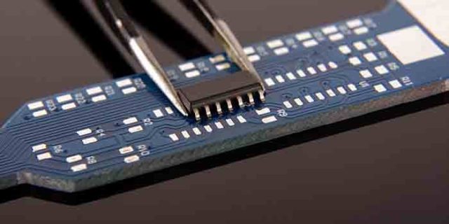
5G module PCB assembly refers to the SMT and assembly process used to integrate baseband chips, RF transceivers, power management ICs, antennas, and passive components onto high-frequency and high-speed PCBs designed for 5G communication.
These assemblies typically involve:
-
High-speed digital signals
-
RF and microwave signal paths
-
Fine-pitch and high-density components
-
Multilayer and high-frequency PCB materials
Key Challenges in 5G Module PCB Assembly
RF Performance Preservation
Maintaining RF performance during assembly is critical. Improper soldering or layout distortion can degrade antenna efficiency and RF signal integrity.
High-Speed Signal Integrity
5G modules operate with extremely high data rates, requiring controlled impedance, minimal skew, and low crosstalk throughout the assembly process.
High-Density and Fine-Pitch Assembly
5G module PCB assembly often involves:
-
Fine-pitch BGAs
-
QFNs and LGA packages
-
Miniature RF components
This demands high-precision SMT placement and reflow control.
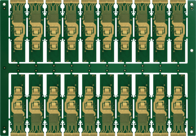
PCB Materials Used in 5G Module Assembly
Professional 5G module PCB assembly supports various advanced materials, including:
-
Rogers RO4003 / RO4350
-
Taconic RF series
-
PTFE-based laminates
-
Hybrid RF + FR-4 stackups
Material compatibility and thermal control are essential during assembly.
SMT Process Requirements for 5G Module PCB Assembly
A reliable 5G module PCB assembly process includes:
-
High-accuracy pick-and-place equipment
-
Optimized solder paste printing
-
Controlled reflow profiles for RF materials
-
Nitrogen reflow for improved solder quality
These processes ensure consistent electrical and mechanical performance.
Testing and Inspection for 5G Module PCB Assembly
Testing is a critical part of 5G module PCB assembly, including:
-
AOI (Automated Optical Inspection)
-
X-ray inspection for BGA and LGA components
-
In-circuit testing (ICT)
-
Functional testing for RF and high-speed signals
Advanced testing ensures each assembled module meets performance requirements.
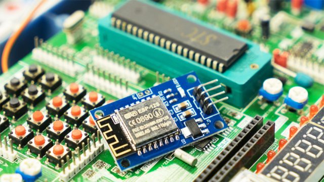
Applications of 5G Module PCB Assembly
5G module PCB assembly is widely used in:
-
5G communication modules
-
IoT and industrial 5G devices
-
5G CPE and gateway systems
-
Automotive and smart infrastructure
-
Wireless networking equipment
These applications demand high reliability and stable RF performance.
Choosing a Partner for 5G Module PCB Assembly
When selecting a supplier for 5G module PCB assembly, consider:
-
Experience with RF and high-speed PCBA
-
Support for high-frequency PCB materials
-
Precision SMT and BGA assembly capability
-
RF testing and functional verification
-
Ability to scale from prototype to mass production
An experienced partner reduces risk and accelerates time to market.
Conclusion
5G module PCB assembly requires advanced SMT processes, RF-aware manufacturing, and comprehensive testing to ensure stable performance. By partnering with a professional PCB assembly provider, manufacturers can achieve reliable, scalable, and high-performance 5G module production.
High-quality 5G module PCB assembly services are essential for meeting the demanding requirements of modern 5G communication systems.
