What Is a 5G IC Test PCB?
A 5G IC Test PCB is a specialized printed circuit board used to test 5G-related integrated circuits, including RF transceivers, baseband chips, power amplifiers, and mmWave ICs. It serves as the critical interface between the device under test (DUT) and automated test equipment (ATE), ensuring accurate electrical and RF performance validation.
Due to the extreme frequencies and bandwidths involved in 5G technology, these test PCBs must meet much stricter electrical and mechanical requirements than conventional IC test boards.
Why 5G IC Testing Is More Challenging
5G ICs operate at sub-6 GHz and mmWave frequency bands, introducing new challenges during testing, such as:
-
High insertion loss at elevated frequencies
-
Signal reflections and impedance mismatches
-
Crosstalk between densely routed RF and digital signals
-
Phase noise and timing instability
-
Power integrity issues under high-speed switching
Accurate 5G IC testing depends heavily on the quality of the test PCB.
Key Requirements of 5G IC Test PCBs
A reliable 5G IC test PCB must provide:
-
Tight impedance control for RF and high-speed digital signals
-
Low-loss transmission paths for sub-6 GHz and mmWave frequencies
-
Excellent signal integrity and phase stability
-
Minimal crosstalk and EMI
-
Stable power distribution networks (PDN)
-
High pin count and fine-pitch support
Even minor PCB variations can significantly affect test accuracy at 5G frequencies.
High Frequency and mmWave PCB Design Considerations
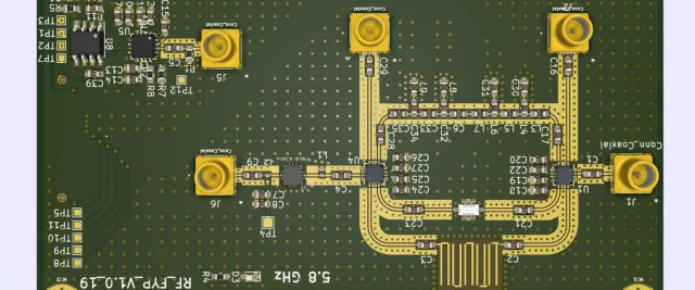
Designing a 5G IC test PCB typically involves:
-
Optimized multilayer stackups with dedicated RF layers
-
Continuous reference planes for impedance stability
-
Short and matched RF trace routing
-
Controlled via transitions and back-drilling where required
-
Isolation techniques between RF, digital, and power domains
-
Proper grounding and shielding structures
Advanced design techniques are essential to ensure repeatable and reliable test results.
Materials for 5G IC Test PCBs
Material selection is critical for high-frequency performance. Common materials include:
-
Low Dk / Low Df laminates for reduced signal loss
-
PTFE-based materials for mmWave applications
-
Hybrid stackups combining RF materials with high-speed digital cores
-
Stable dielectric systems to maintain impedance consistency
Choosing the right materials directly impacts measurement accuracy and yield.
Manufacturing Capabilities for 5G Test PCBs
5G IC test PCBs require advanced fabrication capabilities, such as:
-
Multilayer PCB manufacturing (often 10–30+ layers)
-
Precision impedance control and verification
-
HDI technology for dense routing and fine features
-
High-accuracy drilling and layer registration
-
Premium surface finishes like ENIG or ENEPIG
Manufacturing precision is essential for high-frequency repeatability.
Assembly for 5G IC Testing
Assembly quality is equally critical and typically includes:
-
High-frequency test sockets or DUT interfaces
-
RF connectors and mmWave interfaces
-
Precision passive components
-
Controlled soldering processes to minimize parasitics
A well-controlled assembly process ensures consistent RF performance across test cycles.
Applications of 5G IC Test PCBs
5G IC test PCBs are widely used in:
-
5G RF transceiver and baseband IC testing
-
mmWave IC validation
-
Power amplifier and front-end module testing
-
Network infrastructure and data center IC testing
-
Automotive and industrial 5G electronics
They play a key role throughout IC development, validation, and production testing.
Why Choose a Professional 5G IC Test PCB Manufacturer
An experienced 5G test PCB manufacturer provides:
-
Expertise in high-frequency and mmWave PCB technology
-
Proven material and stackup solutions
-
Stable quality for repeated semiconductor test cycles
-
Fast prototype and small batch production
-
Engineering support from design to final assembly
The right partner helps ensure accurate test results, faster debugging, and shorter time to market.
