// Through-Hole PCB AssemblyHigh-Precision THT PCB Assembly for All Industries
KKPCB provides professional through-hole (THT) PCB assembly services that ensure strong mechanical bonding and stable soldering quality. Our process strictly follows standard operating procedures (SOP), with workstations organized by material classification and operators trained to meet precise process requirements. Throughout the assembly process, engineers and quality inspectors continuously monitor and guide production to ensure consistency and reliability.
We offer both manual insertion for complex assemblies or prototypes and automated insertion for small- and medium-volume production. As a trusted manufacturer of through-hole PCB assemblies, KKPCB delivers cost-effective prototyping, small-batch, and mass production solutions, integrating THT and SMT assembly within one complete turnkey service.
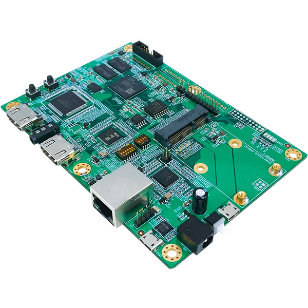
HDMI Extender Through Hole PCB Assembly
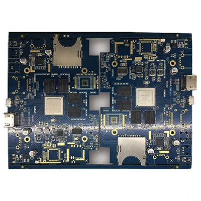
Netcom Prototype PCB Assembly
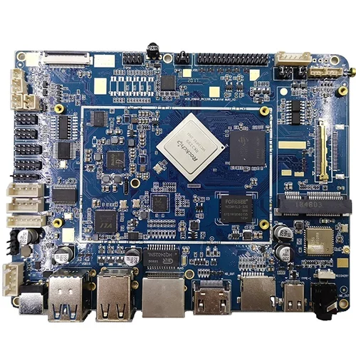
Touch screen motherboard assembly
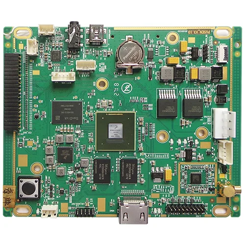
Industrial control motherboard assembly
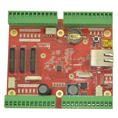
Remote Control System PCB Assembly
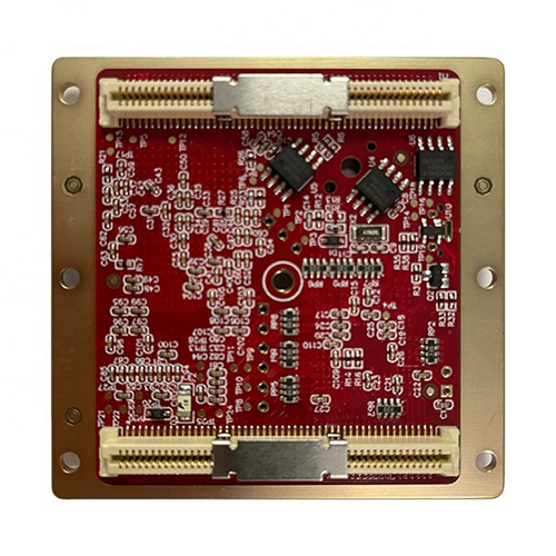
Through Hole PCB Assembly
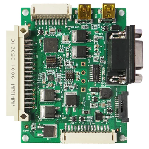
Industrial Control Through Hole PCB Assembly
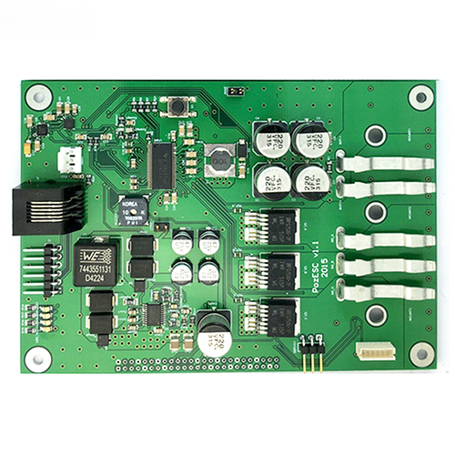
Medical Device Through Hole PCB Assembly
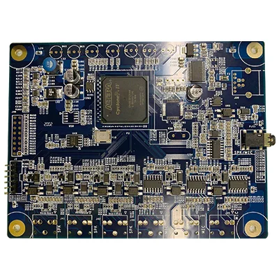
Communication equipment PCB assembly
// Through-Hole Technology (THT) Assembly ServicesThrough Hole PCB Assembly Services
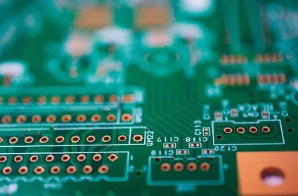
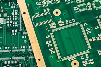
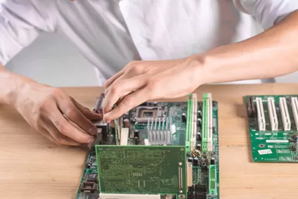
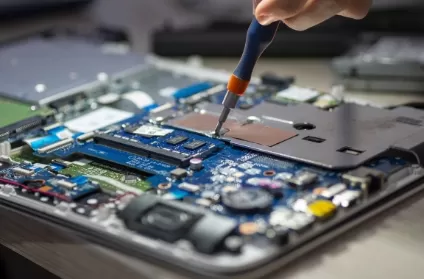
01Through hole PCB assembly process
The broad steps involved in the manual and automated through-hole assembly include:
- Preparing the bare board.
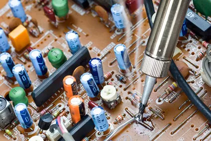
- Manual or automated insertion of components. High speed installation requiresspecialized equipment that can place components axially or radially, as per the design requirements.
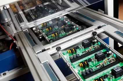
- Using reflow oven to fix soldering paste appropriately.
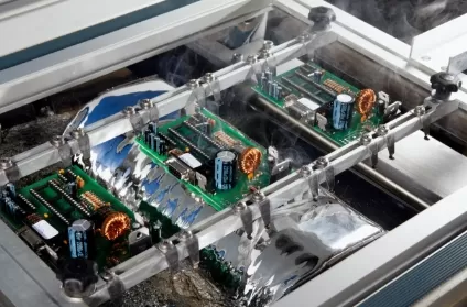
- Manual or automated wave soldering to precisely solder through-hole components.
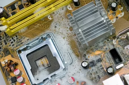
- The use of advanced aqueous washing systems to remove any contaminants from the circuit boards.
- Detailed inspection using different inspection tools and techniques, such as automated optical inspection, X-ray inspection and more.
- Conformal coating as well as device programming, where needed.
- Shipping and Delivery of final through hole PCB assembly.
02Through Hole PCB Assembly Testing Capabilities
- In-Circuit Testing:Widely in use for high volume production lines, they help check the soldering and components.
- Automated Optical Inspection:With this inspection, you can rest assured that there are no soldering or component defects.
- Automated X-Ray Inspection (AXI):Known to improve the quality of through-hole circuit, it inspects for short circuits, fills and more.
- Burn-in Tests:These tests are crucial in that they test the reliability of the PCB in the real time environment.
- Assisted Visual Inspection:Visual inspection by experts helps check accuracy of soldering as well as placement of components.
The above robust testing methodologies will ensure that you receive error free PCBs and that you do not need to deal with costly errors at a later stage when your product has hit the market.
03Through Hole PCB Assembly Capabilities
At KKPCB, we have the following through-hole assembly capabilities:
- Manual and automated insertion of Components
- Hand Soldering
- Double Wave Flow Solder
- Selective Solder
- Legacy Assembly or RoHS Soldering
- Inspection and functional testing
- Conformal Coating
- Device Programming
| Specifications | |
|---|---|
| Components | Connectors and terminals, BGA, μBGA, QFN, Leadless chips, Fine pitch down to 8 mil |
| Board Types | Copper core boards, Aluminum boards, Rigid-flex boards, Rigid FR-4 boards |
| Board Shape | Slots and cutouts, Rectangular, Complex and irregular, Round |
| Assembly Process | Lead-based process, Lead-free (RoHS) process |
| Board Size | Maximum size: 15″ x 20″, Minimum size: 0.2″ x 0.2″ |
| Project File Format | Centroid (Pick-N-Place/XY file), Bill of Materials (BOM) (.xls, .csv, .xlsx), Gerber RS-274X |
04Industrial Applications of Through Hole PCB Assembly Services
Through Hole PCB Assembly finds extensive application in industries where the application needs to bear extreme acceleration, high temperature, high voltage, collision and more. Besides this, through hole assembly is also suitable for testing and prototyping where manual adjustments are required. The industries include:
- Automotive
- Aerospace
- Military
- Medical
- Electronics
- Telecommunication
- Energy
Compliance with highest industry standards
By adhering to ANSI/J-STD-001 and IPC-A-610-D standards, our PCBs meet industry benchmarks for quality. Moreover, our company is certified under ISO 9001:2015, attesting to our commitment to excellence. Dealing with us, you can be assured of receiving only the best, allowing you to enjoy complete peace of mind.
Quick turnaround time
Equipped with automatic insertion equipment for high-speed installation of through-hole components and wave soldering systems, we offer a quick turnaround time that significantly enhances your go-to-market plans.
Error free through hole PCB
With our computer-controlled selective soldering machines, we ensure that we offer you error free PCBs, irrespective of whether you need tin-lead or RoHS through-hole assembly. Our stringent testing and inspection capabilities mean any errors are weaned out early and you do not have to deal with costly errors later.
// Frequently Asked Questions (FAQ)Through Hole PCB Assembly (FAQ)
Through-hole PCB assembly involves inserting electronic components into pre-drilled holes in a PCB and soldering them on the opposite side, creating strong electrical and mechanical connections. This method is valued for its durability and is commonly used in applications requiring robust connections, such as automotive, aerospace, and military electronics. While it provides strong mechanical support, it requires more space on the PCB and limits component density compared to surface-mount technology (SMT).
For one, it offers reliability on account of the stronger bonds between the components and the board. It is also preferred for large components and in applications that undergo environmental stress. Their durability also makes them a good choice for prototyping.
yes, you can count on us for both legacy and RoHS assembly. We handle legacy assembly by working with older components and technology while ensuring they are correctly integrated into your PCB design. For RoHS assembly, we adhere to strict environmental regulations by using lead-free solder and materials to meet RoHS compliance standards. Whether you need support for older designs or require compliance with modern environmental standards, we offer expertise and solutions to meet your specific assembly needs.
Yes, we offer prototype quantities for through-hole PCB assemblies. We understand the importance of validating designs and functionality with smaller production runs before scaling up. Whether you need a few prototypes for testing or initial runs for validation, we can accommodate your requirements with high-quality assembly services tailored to your prototype needs.
Yes, we undertake assembly rework. Our services include correcting defects or issues in assembled PCBs, such as fixing soldering problems, replacing faulty components, or addressing design changes. We use advanced techniques and equipment to ensure that the rework is performed to high standards, maintaining the integrity and functionality of the final product. If you encounter any issues with your PCB assembly, we are equipped to handle rework efficiently and effectively.
Yes, we offer quick delivery for through-hole circuit board assembly. We understand the importance of timely project completion and strive to provide fast turnaround times without compromising quality. Our quality assurance processes include thorough inspections and testing to ensure that each assembly meets high standards. We are committed to delivering reliable and high-quality assemblies even with expedited timelines.
KKPCB is a trusted partner for industrial through-hole PCB assembly thanks to our deep expertise, advanced production technology, and rigorous quality control. We deliver reliable, high-performance boards tailored to your exact specifications while maintaining fast turnaround times. Our manufacturing process follows strict IPC standards, and every assembly undergoes thorough inspection to ensure long-term stability. Backed by responsive customer support and years of experience in industrial electronics, KKPCB guarantees consistent quality and dependable service for all your through-hole PCB requirements.

