// High-Precision SMT PCB AssemblyAdvanced Surface Mount Technology for Reliable Prototypes and Production
At KKPCB, we operate state-of-the-art SMT assembly lines designed for precision, reliability, and speed. Our advanced production systems ensure consistent quality and faster turnaround for both prototype and production runs.
We handle single- and double-sided SMT assemblies for a wide range of component types, including:
-
Ball Grid Array (BGA)
-
Ultra-Fine Ball Grid Array (uBGA)
-
Quad Flat Pack No-Lead (QFN)
-
Quad Flat Package (QFP)
-
Small Outline Integrated Circuit (SOIC)
-
Plastic Leaded Chip Carrier (PLCC)
-
Package-on-Package (PoP)
-
Small Pitch Components down to 0.2 mm
To guarantee the highest level of accuracy and reliability in high-density SMT PCB assemblies, we apply multiple testing and inspection processes, including:
-
Automated Optical Inspection (AOI)
-
X-ray Testing
-
In-Circuit Testing (ICT)
-
Functional Testing
Through rigorous process control and advanced inspection technologies, KKPCB ensures zero-defect performance and production-ready PCB assemblies for demanding industries such as automotive, telecommunications, medical, and industrial automation.
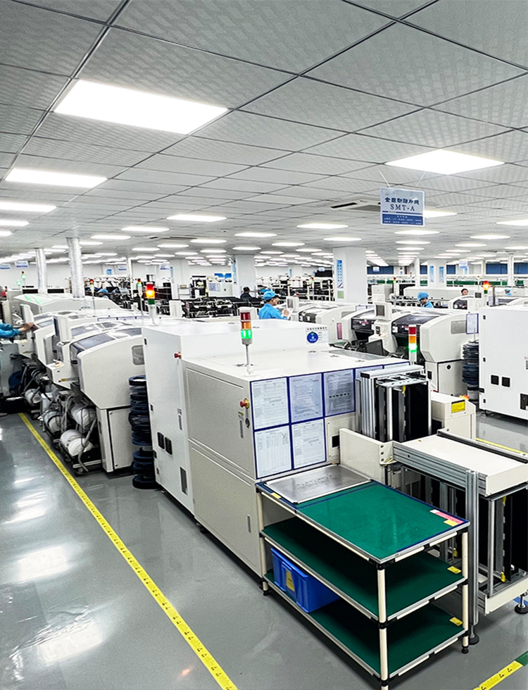
// High-Precision SMT PCB AssemblyAdvanced Surface Mount Technology for Reliable Prototypes and Production
KKPCB provides professional SMT PCB assembly services powered by advanced automated production lines equipped with high-speed pick-and-place machines, precision reflow soldering, AOI, X-ray, and ICT inspection systems. We specialize in high-density and fine-pitch component assembly including BGA, QFN, CSP, PoP, and ultra-small 01005 packages, ensuring unmatched accuracy and consistency in every build. Through comprehensive DFM analysis and process optimization, we achieve excellent yield and reliability even for complex SMT designs. With flexible production capabilities covering prototypes, small, and medium-volume runs, KKPCB serves clients across industrial control, automotive, telecommunications, medical, and IoT industries. By integrating strict process control, full material traceability, and ISO/IATF-certified management, we guarantee zero-defect quality, rapid turnaround, and long-term reliability—helping customers accelerate time-to-market with confidence and precision.
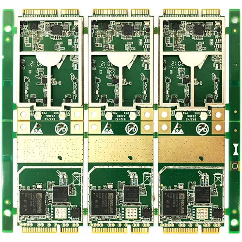
communication module SMT patch
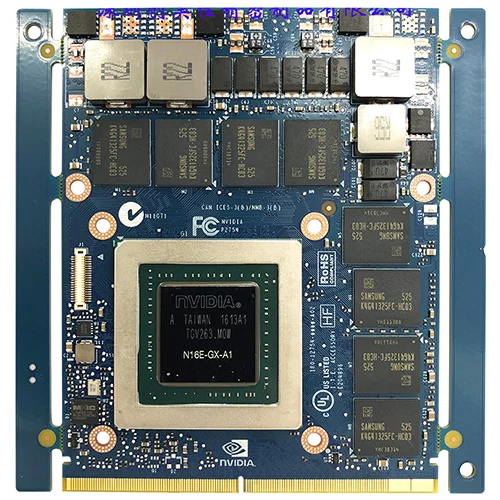
Gaming graphics card SMT assembly
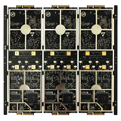
Communication module SMT Assembly
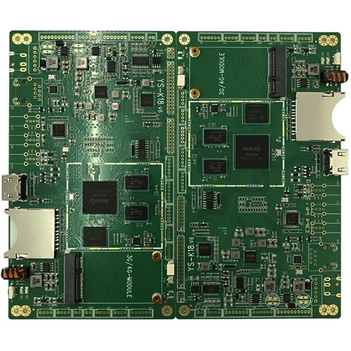
Industrial control SMT PCB Assembly
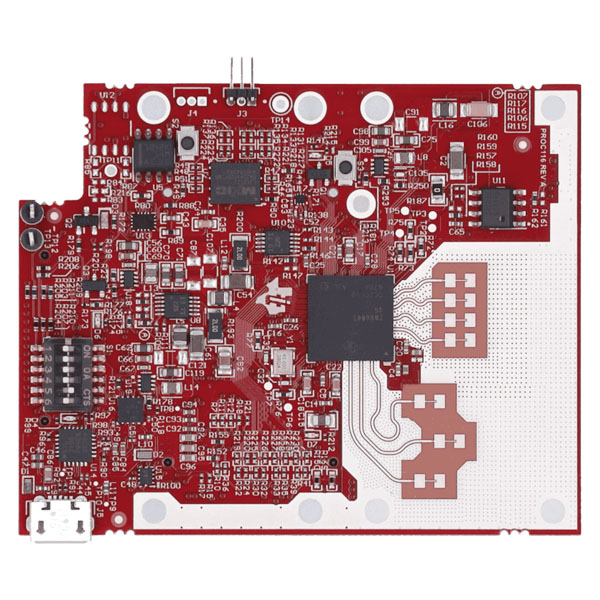
mmWave Hybrid PCB Assembly
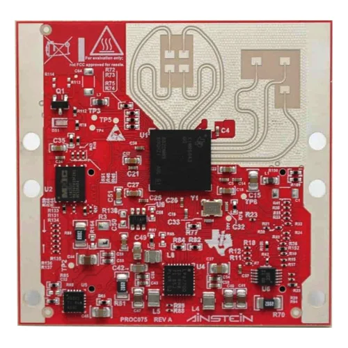
mmWave sensing device PCB Assembly
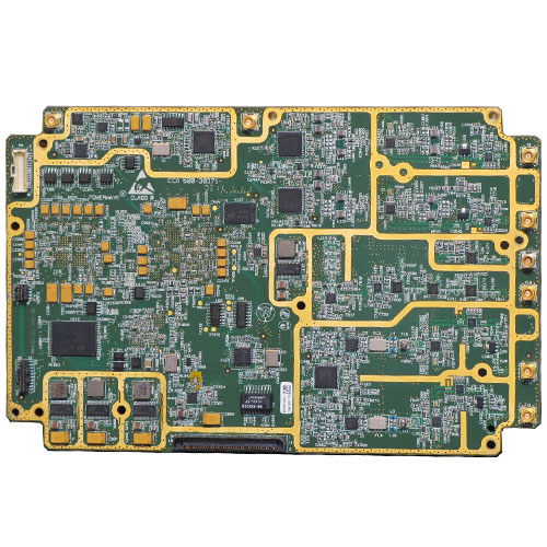
Military Applications RF PCB Assembly
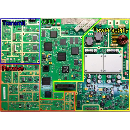
RRU3908 base station PCB Assembly
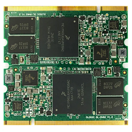
Core motherboard SMT PCB Assembly
// PCB SMT ServicesOne-Stop Solution for High-Precision SMT PCB Assembly
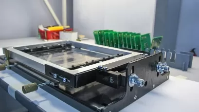
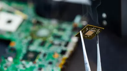
01SMT PCB assembly capabilities
| Juki JX-100 SMT Pick & Place Machine | |
|---|---|
| Technical Specifications | 6 heads with laser alignment, 14,400 components per hour, small chip 8 mm or smaller Placement points per program: 2000 |
| Supported Component Sizes | Height: min 0.3 mm, max 6 mm Size: min 0.75 x 0.5 mm, max 33.5 mm² Lead pitch: 15 mil |
| Supported PCB Sizes | Min: X 50 mm x Y 30 mm Max: X 330 mm x Y 250 mm Thickness: min 0.4 mm, max 4 mm |
| Zevatech FS-750 SMT Pick & Place Machine | |
|---|---|
| Technical Specifications | 3 heads with laser alignment, 8,000 components per hour, small chip 8 mm or smaller Placement points per program: 2000 |
| Supported Component Sizes | Height: min 0.3 mm, max 6 mm Size: min 1.0 x 0.5 mm, max 23.5 mm² Lead pitch: 15 mil |
| Supported PCB Sizes | Min: X 50 mm x Y 30 mm Max: X 330 mm x Y 250 mm Thickness: min 0.4 mm, max 4 mm |
| Zevatech PM-570 SMT Pick & Place Machine | |
|---|---|
| Technical Specifications | 1 head with laser alignment, 3,870 components per hour, maximum rating Placement points per program: 2000 |
| Supported Component Sizes | Height: max 6 mm Size: min 1.0 x 0.5 mm, max 33.5 mm² Lead pitch: 15 mil |
| Supported PCB Sizes | Min: X 30 mm x Y 30 mm Max: X 406 mm x Y 330 mm Thickness: min 0.6 mm, max 2.5 mm |
02SMT PCB assembly services for various industries
As Surface Mount Technology (SMT) continues to advance, its adoption has rapidly grown across a wide range of industries. Today, SMT PCB assembly services are increasingly critical for applications requiring precision, reliability, and high-density component placement.
Industries we serve include:
-
Aerospace & Defense
-
Consumer Electronics
-
Medical & Healthcare
-
Transport & Automotive Electronics
-
Telecommunication & Mobile Communications
-
LED & Lighting Components
At KKPCB, we provide comprehensive SMT PCB assembly solutions covering all assembly types and PCB sizes—from traditional through-hole assembly to standard SMT and ultra-fine pitch BGA assembly. Our services are flexible, supporting prototype, small, medium, and large-volume production, and accommodating single- or double-sided SMT assembly for all component types. Wave soldering and advanced assembly techniques are performed using cutting-edge equipment in fully ESD-controlled areas, ensuring maximum reliability and quality.
Our SMT assembly capabilities include:
-
Complete SMT assembly lines with automated pick-and-place and reflow soldering systems
-
Single and double-sided PCB assembly
-
Low to high-volume production
-
Strict ESD-controlled manufacturing environment
-
Full inspection and quality control, including AOI, X-ray, and functional testing
We specialize in high-density, ultra-compact component placement, capable of handling:
-
Smallest packages: 01005, 0201, 0402
-
Fine-pitch components down to 0.25 mm
-
Leadless components, BGA, µBGA, LGA, Package-on-Package (PoP), and other advanced packages
With KKPCB’s SMT assembly services, customers across diverse industries can rely on precision, reliability, rapid turnaround, and scalable production, accelerating their product development while maintaining uncompromising quality.
03SMT Assembly Advantages
Surface-mount technology (SMT) assembly has several advantages over traditional through-hole technology. Here are some of the main advantages of SMT assembly:
1. Space-saving
SMT components are much smaller than through-hole components, which allows for much denser circuitry and smaller PCBs.
2. Faster assembly
SMT components can be placed on a PCB much more quickly than through-hole components, as they can be placed and soldered using automated equipment.
3. Lower cost
SMT assembly is generally less expensive than through-hole assembly, as it requires less manual labor and can be automated more easily.
4. Higher reliability
SMT components are less prone to mechanical stress and vibration, as they are mounted directly on the surface of the PCB.
5. Smaller footprint
As SMT components are much smaller than through-hole components, they take up less space on a PCB, which allows for more compact designs.
6. Weight advantages
SMT components are lighter in weight than through-hole components, which can be an important consideration for applications where weight is a concern, such as in aerospace or portable electronic devices.
04SMT Assembly Testing Capabilities
We make it mandatory for ourselves to perform visual inspections to ensure that there are no missing or misaligned components or issues with solder bridging. In addition to manual inspections, we also use SMT inspection machine to guarantee thoroughness. If we detect any fault during this rigorous inspection process, we immediately send the board back for rework. Once the rework is completed, we again test the boards to verify if everything is working correctly. We take pride in our strict quality control measures and make sure that each board meets our high standards before delivering it to our customers.
We make sure no mistake has been made and that all parts are in the right place by using an AOI machine. As the 3D technology rolled out, we also started going for it instead of 2D inspection and avoided any false calls. With 3D inspection, we go for accurate measurements for a more stable inspection process.
Different Testing Services during SMT Assembly
Automated Optical Inspection
For pre- and post-solder to identify the component presence, placement, and solder quality.
After the component placement, we perform an automated optical inspection to make sure that all the components are mounted in the right place. We use AOI equipment for verifying the components’ placement, orientation, and polarity.
We also perform a post-reflow AOI to make sure no mistakes are made and then we perform an X-ray inspection for the process verification.
X-ray Testing
We go for this test to check on leadless components through an x-ray image of them and the solder joints to make sure that everything is working as expected.
In-circuit Testing
Through this, we look for any joint failures and we perform this through bed-of-nails tests.
Functional Testing
We perform this to ascertain PCBs will work productively and as per the requirements after the SMT assembly. With testing, we ensure the quality of delivered range of SMT PCB assemblies.
// KKPCB Rapid SMT Assembly ServiceWhy Work with Us for SMT Assembly?
// Frequently Asked Questions (FAQ)SMT PCB Assembly (FAQ)
SMT process reduces manufacturing costs and also makes efficient use of the PCB space. Through effective utilization of SMT, we are able to build highly intricate electronic circuits onto miniature and smaller assemblies by relying on automation. Essentially, you can have the following with SMT –
- Smaller PCB Size
- Higher component density
- Fewer drilling holes
- Lower cost
- Faster production time
- Reliability as solder joint formation is more reliable
- Stable and high performing even in shaky conditions
SMT assembly types include –
- Ball Grid Array (BGA)
- Ultra-fine Ball Grid Array
- Small Outline Integrated Circuit
- Plastic Leaded Chip Carrier (PLCC)
- Small Chip Packages (SOP)
- Quad Flat Package (QFP)
- Quad Flat Pack No-Lead (QFN)
- Package on Package (POP)
In consumer electronics devices like tablets, mobile phones, there is a need for compact assembly of components onto the printed circuit boards. Here, SMT can be effectively used to make the best and optimum use of the available space. This process also builds lightweight products as there is no need for extra wiring and soldering.
Choosing KKPCB for SMT PCB assembly offers advantages such as extensive expertise, advanced technology, and rigorous quality control. We provide customized solutions, fast turnaround times, and strong customer support, ensuring high-quality and reliable results for your electronic assembly projects.
SMT (Surface-Mount Technology) and through-hole technology differ primarily in mounting methods and assembly processes. SMT involves placing components directly on the PCB surface and is favored for its high component density, compact design, and efficiency in high-volume production. Through-hole technology, on the other hand, requires components to pass through holes in the PCB and is valued for its strong mechanical connections and suitability for simpler designs or prototypes. SMT generally offers faster assembly and greater design flexibility, while through-hole technology provides robust mechanical support and is better for applications with significant physical stress.
The current trend is automation. So, we follow the same cue. The majority of the SMT parts on your circuit boards will be assembled with automated pick-and-place equipment.
Even though we rely on automated assembly processes, some components cannot be placed.
- Components that are lightweight
- Those that have too much heat sensitivity
- Lack of robust solder joints
- Damaged components
To start the SMT process, we need the components and raw boards to prepare them for production. These things would be validated by your Contract Manufacturer (CM)’s inspection teams to make no mistakes.

