The thermal conductivity of a printed circuit board (PCB) is largely determined by the properties of its dielectric layers, such as FR-4, high-TG materials, or thermally enhanced laminates.
In low-power and high-reliability electronic devices, efficient thermal management is still critical to ensure long-term performance and stability.
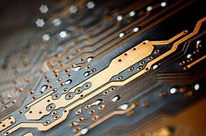
To improve heat dissipation, PCB designers commonly use thermal via arrays to transfer heat from surface components to inner or bottom copper layers. However, designing the most effective thermal via array configuration is a complex engineering challenge, involving material selection, via geometry, layout density, and manufacturing constraints.
At KKPCB, we provide advanced PCB thermal design and manufacturing solutions to help customers optimize heat dissipation without increasing cost or board complexity.
1. Key Factors Affecting PCB Thermal Conductivity
1.1 Dielectric Material Properties
The base material of the PCB plays a dominant role in thermal performance:
| Material Type | Typical Thermal Conductivity (W/m·K) |
|---|---|
| Standard FR-4 | 0.3 – 0.4 |
| High-TG FR-4 | 0.4 – 0.6 |
| Thermally Enhanced FR-4 | 1.0 – 3.0 |
| Metal Core PCB (MCPCB) | > 2.0 |
Even with advanced laminates, vertical heat transfer through dielectric layers remains limited—this is where thermal vias become essential.
2. Why Use Thermal Via Arrays in Low-Power PCB Design?
Although low-power devices generate less heat, localized hotspots around ICs, regulators, and RF modules can still impact:
-
Component lifespan
-
Signal stability
-
Overall system reliability
Thermal via arrays provide a low-resistance heat path by conducting heat through copper-plated holes into internal ground or power planes.
Advantages of thermal vias:
-
Improved heat spreading
-
Reduced junction temperature
-
No additional board area required
-
Compatible with standard PCB manufacturing
3. Thermal Via Array Design Parameters
3.1 Via Diameter and Aspect Ratio
-
Typical thermal via drill size: 0.2–0.4 mm
-
Smaller vias allow higher density but increase manufacturing difficulty
-
Lower aspect ratio improves copper plating quality
3.2 Via Quantity and Spacing
-
Increasing the number of vias reduces thermal resistance
-
Excessively dense vias may:
-
Increase PCB cost
-
Affect solder joint reliability
-
-
Recommended via pitch: 0.8–1.2 mm
3.3 Via Filling Options
| Via Type | Thermal Performance | Cost |
|---|---|---|
| Open via | Medium | Low |
| Resin-filled via | High | Medium |
| Copper-filled via | Very high | High |
At KKPCB, we help customers select the optimal via filling method based on thermal requirements and cost targets.
Thermal vias are most effective when connected to large internal copper planes, such as:
-
Ground planes
-
Dedicated thermal planes
-
Power distribution layers
Stack-up considerations:
-
Thicker copper layers (2 oz or more) improve heat spreading
-
Symmetrical stack-ups reduce warpage during reflow
-
Thermal simulation during PCB design phase is highly recommended
5. Why Thermal Via Optimization Is a Complex Task
Designing an effective thermal via array is not just about “adding more vias.” Engineers must balance:
-
Thermal performance
-
Electrical integrity
-
Mechanical reliability
-
Manufacturability
-
Total PCB cost
This is why early collaboration between PCB designers and manufacturers is essential.
At KKPCB, our engineering team supports:
-
Thermal simulation review
-
Via array optimization
-
Material selection guidance
-
DFM (Design for Manufacturability) analysis
6. KKPCB Thermal Management Solutions
KKPCB offers one-stop PCB thermal design and manufacturing services, including:
-
Multilayer PCB with optimized thermal vias
-
High-TG and thermally enhanced materials
-
Resin-filled and copper-filled vias
-
Low-power and high-reliability PCB solutions
Whether your project involves consumer electronics, industrial control, or RF applications, KKPCB ensures stable thermal performance and consistent quality.
While the thermal conductivity of PCB dielectric materials sets the baseline for heat transfer, thermal via arrays are the most practical and cost-effective solution for improving heat dissipation in low-power PCB designs.
However, achieving optimal performance requires careful consideration of via geometry, density, stack-up, and manufacturing processes.
Partner with KKPCB to transform complex thermal challenges into reliable, manufacturable PCB solutions.
