// PCB PROTOTYPING SERVICESHigh-Quality Prototype PCB Manufacturing
KKPCB is a professional prototype PCB manufacturer serving innovative companies across design, industrial, medical, and equipment manufacturing sectors. With decades of experience, our team continuously leverages advanced technologies and methods to enhance prototype quality and reduce production lead times. We provide specialized prototype PCBs from 2 to 58 layers, using the same cutting-edge equipment, materials, and processes as our standard PCB production, delivering cost-effective solutions without compromising the high quality you expect from a leading Chinese PCB manufacturer.
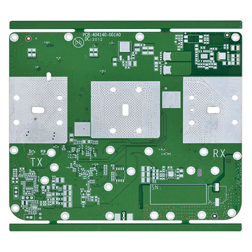
6-layer communication PCB board
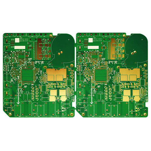
8-layer energy device PCB prototype
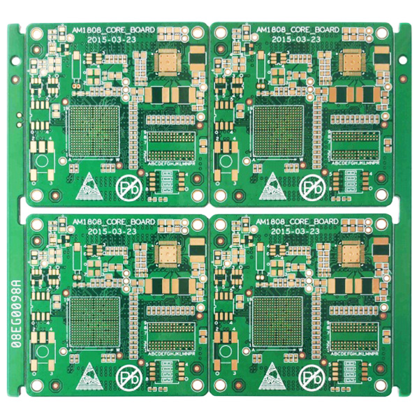
12-layer PCB prototype manufacturer
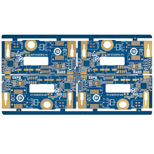
6-layer industrial control prototype PCB
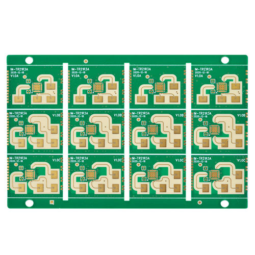
Communication equipment PCB prototype
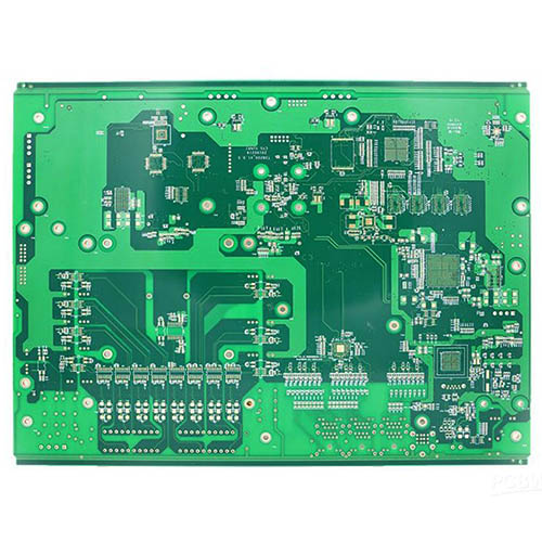
Core motherboard PCB
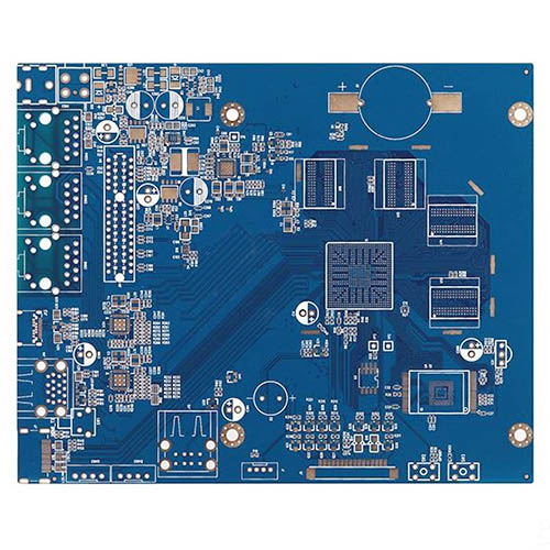
Medical video capture card PCB
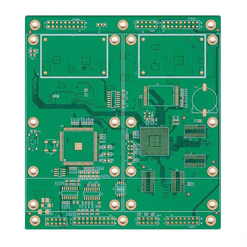
8-layer industrial control system PCB
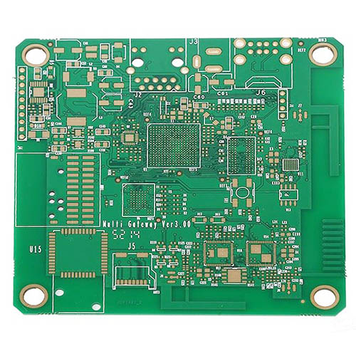
Standard PCB Prototype Manufacturer
Our quick turnaround PCB services include:
-
PCB Prototype Assembly
-
Rigid-Flex PCBs
-
HDI SBU PCB Fabrication
-
Flexible PCBs
-
PTFE Teflon PCBs
-
Heavy-copper PCBs
-
Metal Core PCBs
-
High Frequency-Antenna PCBs
-
BGA Pad pitch down to 0.15mm
-
Cavity Process
-
Back drill Process

Why Choose KKPCB as your Rapid Prototyping Manufacturer?
Select KKPCB as your rapid prototype manufacturer for a seamless experience. Our commitment to quality and efficiency ensures your project’s success. We offer high-end equipment, experienced engineers, and aligned production. All these factors can turn your designs into functional prototypes .
We have a proven history of being accurate and dependable. Choose us to make your ideas come true. From PCB design to rapid assembly, we provide end-to-end services. So, choose KKPCB for cost-effective prototyping.
Custom PCB Service
We have fifteen years of custom PCB manufacturing experience. Our experienced engineering team created our advanced machines. They meet a variety of high-difficulty and high-precision PCB manufacturing.
We keep the complete set of precision automation equipment. We keep Universe VCP, advanced laser /mechanical drilling, and automatic silkscreen exposure machines. Also, we have LDI high-precision exposure and AOI machines. These top-notch automation equipment provide high-quality guarantees for customers.
Select High-End Materials
Selecting reliable brand materials ensures product quality and controls the production process. Standard material are FR4 (Shengyi, ITEQ, KB, Nanya). High-frequency materials are Rogers、Taconic、Nelco、Arlon 、Isola、F4B、TP-2. High-Tg materials are Shengyi S1000‐2, S1170, KB. Halogen-free materials are EMC EM285, EM370(D), Shengyi S1155、S1165.
Leading PCB Production Capacity
We can have up to 48 layers in our design. The maximum weight of copper is 10 ounces. The smallest size for mechanical drill holes is 0.1mm with an accuracy of +/- 0.05mm. We have unique methods like controlling impedance and using buried/blind Vias. We also place Vias in the pad and do edge plating. We specialize in half-cut/castellated holes, countersinks/counterbores, and press-fit holes. Moreover, these techniques also include heavy copper, hard gold, custom Stackup, and more.
PCB Quality Management System
When you use the IPC quality management system, you are guaranteed a 100% product qualification rate. All PCB boards are 100% electric tested to provide high-quality PCB board products. Continuous improvement of quantity, technology, and service meets customers’ expectations.
Fast Turn Times Of PCB Prototype
Using an ERP order management system, clear production control ensures on-time delivery. This system also includes a rigorous production process for quick delivery.
The fastest expedited PCB prototype order we can do is 12 hours. We also provide customized PCB orders with 99% On-time delivery.
Security and efficient shipment ensure on-time delivery.
Complete PCB Services
Provide 7×24 hours of technical support for PCB design and PCB manufacturing. One-stop services from design to production significantly shorten the customer’s development cycle. One-to-one VIP service for pre-sales and after-sales.

As an important trial production stage before mass PCB production, the prototype PCB fabrication has an important guiding significance for testing the function of new products. Prototype PCB fabrication can identify product design defects in the early stage, verify product function, and avoid batch scrap. PCB prototyping production in this stage needs rapid turnover, so as to shorten the development cycle of product iteration. This paper introduces the advantages of prototype PCB production and the high difficulty and complex PCB prototype production advantages of KKPCB.
What is PCB Prototype?
In order to correct errors and defects and make the product have perfect functions, we must test the product in advance. The same for PCB. Before the printed circuit board is put into use, it must be ensured that it meets the standard and quality. In fact, despite the best efforts of designers and engineers, small, invisible errors can threaten the function and goal of the final PCB. If you don’t solve these problems, they become expensive and useless.
Before moving into more complex designs, they usually order multiple PCB prototypes runs to test the redesign or test a single function. This enables them to identify elements that need to be corrected early in the process. The earlier these problems are discovered, the lower the cost.
PCB Prototype: also known as a printed circuit board or prototype circuit board, PCB prototype board is widely used, almost all electronic products need PCB prototype and PCB prototype assembly, which leads to the growth of PCB prototype company.
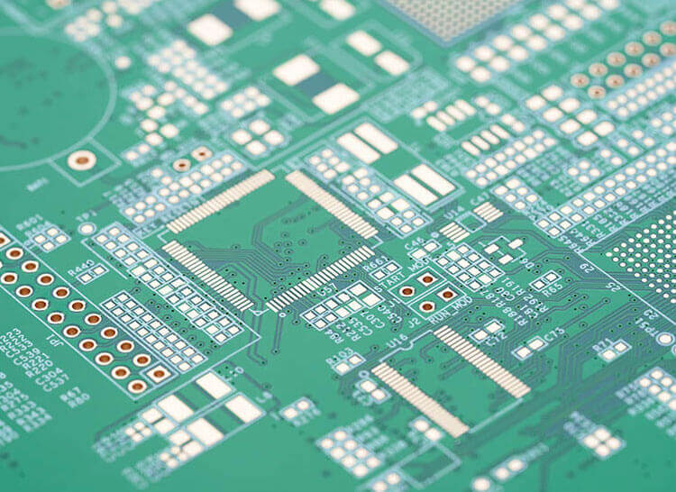
The PCB prototype is developed as a sample of a real PCB to test the design and ideas for an early understanding of the product. PCB modification design needs certain functions. All functions of PCB design are tested by PCB prototype. We use different types and designs of PCB prototypes to test different functions of PCB. Developers can use multi-functional PCB at all stages of the program. This depends on the size of the PCB hole and the thickness of the board.
Why use the PCB prototype?
So why use PCB prototypes instead of standard production runs? This may seem like an extra step, but in the long run, it can save you time and money and produce a better end product.
1. You may go through many design iterations when developing a new PCB-based design. You need to be able to test new designs quickly so that production can be completed in time, as a lengthy design process can lead to loss of revenue. The rapid speed of our prototyping services, combined with testing designs before production runs, can minimize wasted project expenditures and maximize your investment.
Standard production operations will also increase rapidly in terms of costs. The earlier you discover design defects or inefficiencies in a PCB design, the lower the cost of solving the problem. If you don’t use prototype boards to test your design, you may have problems later in the production run – that is, after you’ve invested a lot of money into producing standard PCBs. Our are also suitable for small volume production.
2. Engineers also often use prototype PCBs to test a single function of more complex products containing multiple PCBs. Before adding the next level of functionality, they will order prototypes that perform the most basic functions. If you don’t test the features separately, you may encounter performance problems in subsequent processes, and not sure which board caused the problem. Through the prototype design of each function step by step, a lot of time and resources can be saved.
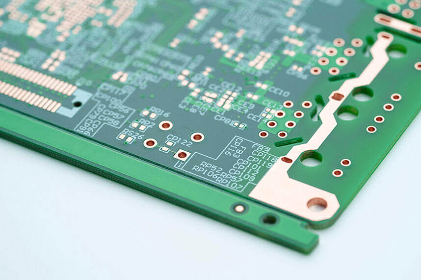
Although prototype PCBs do not allow manufacturing tolerances to be as high as those for standard production runs, they still accurately describe how the final PCB-based solution works. Once you have fully validated your design through the prototype board, you can continue with the standard production run, which has tighter manufacturing tolerances, can handle more functions, and can contain a larger order volume.
As part of our standard production products, we provide DFM to help identify any problems that may affect manufacturing. If we find any potential problems, we will contact you to develop the necessary solutions.
If you are developing new products or redesigning them, you may benefit from our prototype PCB production services. Before you invest a lot of time and money into a project, it will help you discover any potential problems or changes you may want to make to your design. This will raise the bottom line of your project, resulting in a higher quality end product and contributing to its overall success.
What are the advantages of the PCB prototype?
So choosing to order PCB prototypes instead of going directly to standard production runs provides many advantages. In almost any case involving new or updated design, PCB prototype design can prove to be beneficial. The advantages of using our PCB prototyping services include:
Fast turn around time
We can produce PCB prototypes faster than standard production PCB. We can complete the prototype order in just two days. Our standard production board takes 3 to 18 days to build, while our prototype takes only 2 to 5 days to build.
Early detection of defects
Prototyping enables you to catch design defects early in the product development process before you invest too much time and money into problem design. Engineering changes early in the process will avoid a number of potential problems.
Ability to test components individually
It is useful to test different components individually for complex project components involving multiple PCB-based projects. By validating each component individually, you can identify any problems that may occur. Without this, it’s hard to determine where the problem lies.
Accurate representation of standard PCB performance
High-quality PCB prototypes can accurately represent final production mode components. Although the tolerances are low, they still give you an idea of what you expect when you start a standard production run.
Efficient project completion
Use PCB prototypes to identify and correct design defects early, and quickly identify components that need to be adjusted. Failure to do so may significantly extend the time frame of the project, which may result in loss of revenue and customer dissatisfaction.
Reduce overall costs
By helping you find problems faster, it enables you to fix them before you invest in large volume standard production runs. By identifying problems in simpler product versions, you can redesign simpler components without having to build the entire project, which is more expensive.
Improved end products
PCB prototype design helps focus on improving each PCB and component to achieve a higher quality design. It can also help you avoid any undetected faults that may occur in the final product and cause more serious problems.
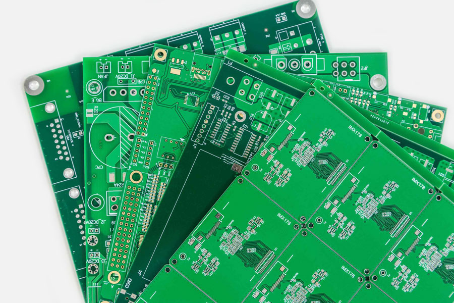
The benefits provided by PCB prototypes are used in most new or revised PCB designs. Once you have verified the functionality that prototypes must provide for the project, you can continue with the standard PCB production run.
PCB Prototype Application
Printed circuit boards that connect components through a variety of related circuits are the core of many different electronic devices we use every day. They have many different variants that enable them to function in a variety of situations. PCB is an integral part of electronic products used in almost all industries. You can find them in consumer electronics, medical equipment, auto parts, industrial equipment, lighting technology, aerospace equipment, etc.
As people continue to innovate and create more new electronic equipment, PCB becomes more common. It is in the development of these new products that the prototype PCB is the most useful.
When to use PCB prototype?
When one of the following situations is involved, prototype design and manufacturing should be considered:
New products – any time your project involves developing a new product, you may not be able to detect any existing problems without prototype design, which can lead to more serious problems or more difficult to fix, enabling you to quickly and economically identify any factors that need to be adjusted.
Quality and design testing – if you want to do quality testing or design review, you should order a PCB prototype. A shorter build time will allow you to start reviewing or testing faster and will lower your overall costs. The PCB prototype will give you an accurate understanding of the performance of the final product.
Complex components – if your project contains multiple PCB-based components, use a PCB prototype. More components may mean more functionality, but more potential failures. Prototyping is particularly useful for these more complex projects because it helps quickly identify which component is not performing correctly. By ordering one PCB at a time, you can spend less time testing and correcting problems and save money.
Ordering PCB prototypes
At KKPCB, we provide a one-stop service for all your PCB prototype design and standard production requirements. We can complete every part of the prototyping process – including component procurement, manufacturing, assembly, and quality control. This way you don’t have to work with multiple PCB vendors to make the process more efficient and economical.
Quick turn PCB prototypes-Shorten your time
Time is crucial in today’s fast-growing industrial life, so it is necessary to follow this factor to save valuable resources. In PCB manufacturing, PCB with a fast turnaround is needed. In the process of quickly starting PCB, ensure that customers get the product within the specified time. A time frame is needed for this. Rapid production of PCB is undoubtedly very important to customers.
- No delay, the product will be delivered on a fixed date
- Save time
- Reduce production cycle
PCB manufacturing is a long process. It will take a few days to develop it. The quick turn PCB reduces the waiting time of PCB shoppers.
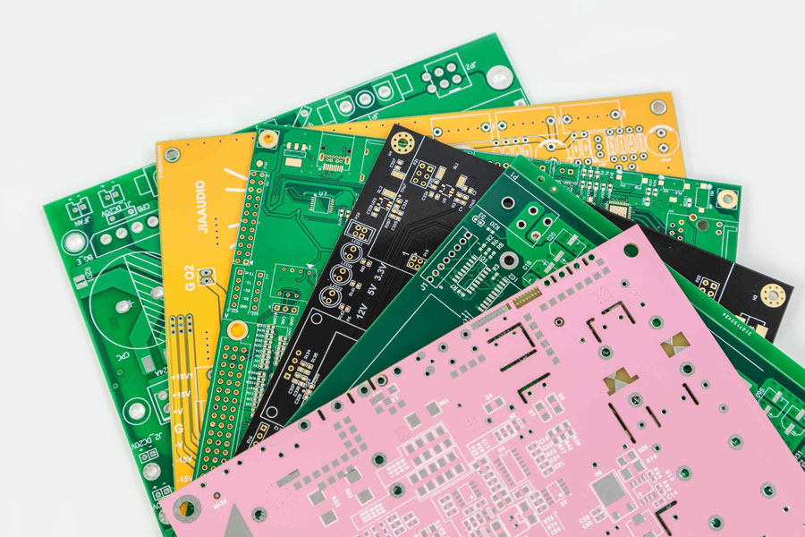
The key point of a rapid manufacturing PCB prototype is to carry out rapid PCB assembly before the final PCB product is complete. In a short time, PCB manufacturing becomes simple and fast. The quick start prototype PCB provides some core solutions for PCB shoppers.
KKPCB is a professional PCB prototype manufacturer. We spend a lot of time and energy updating our production process and technology and strive to provide the best quality PCB prototype service. We mainly produce single board and double board rapid prototyping, multilayer board, aluminum PCB, metal PCB, HDI board, and high-frequency PCB. Most importantly, we provide PCB assembly and component procurement to provide customers with one-to-one best PCB prototype service.
// Frequently Asked Questions (FAQ)PCB prototype FAQ
- Design Verification:
- Functionality: Ensure the PCB performs as intended according to the design specifications.
- Signal Integrity: Test the electrical characteristics of the PCB, including signal integrity, power distribution, and impedance.
- Component Fit: Check the physical fit and placement of components on the PCB.
- Error Detection and Correction:
- Identifying Issues: Detect design flaws, layout errors, and potential manufacturing problems early in the development process.
- Refinement: Make necessary adjustments to the design before committing to mass production.
- Performance Testing:
- Operational Testing: Assess how the PCB operates under various conditions, including load testing, thermal performance, and environmental stress.
- Reliability: Evaluate the durability and reliability of the PCB over time.
- Validation and Certification:
- Compliance: Ensure the PCB design meets industry standards and regulatory requirements.
- Prototyping for Certification: Use prototypes for obtaining certifications, such as UL, CE, FCC, and others, necessary for the product’s market entry.
PCB Prototyping Process
The prototyping of PCBs involves a systematic sequence of steps to ensure the final product meets design requirements and performs reliably. It begins with design preparation, where the circuit schematic is created using CAD software, and the PCB layout—including component placement and routing—is designed. Next is material selection, choosing the appropriate substrate (e.g., FR4, polyimide) and components that match the design specifications.
During fabrication, the PCB is manufactured using standard processes such as etching, drilling, and plating, followed by initial quality control to verify that design tolerances are met. The assembly stage involves placing and soldering components onto the PCB, with thorough inspections for defects like solder bridges or misaligned components.
Testing and validation ensure the PCB functions correctly, including electrical performance checks and environmental testing under varying conditions such as temperature and humidity. Finally, the iteration and refinement stage uses feedback from testing to make design adjustments and, if necessary, produce updated prototypes, ensuring the final PCB meets all performance, reliability, and functionality expectations.
Risk Reduction: PCB prototyping helps detect and address design issues early, minimizing the risk of costly errors during mass production. Iterative testing allows multiple design refinements, ensuring a robust final product.
Cost Savings: By validating the design before full-scale production, prototyping prevents expensive rework and redesigns. It also optimizes the use of materials and resources, making the development process more efficient.
Time Efficiency: Early issue detection accelerates the development cycle, allowing faster resolution of potential problems. A validated prototype ensures a smoother transition to mass production, reducing delays and unexpected setbacks.
Market Readiness: Prototyping facilitates compliance with industry standards and necessary certifications. It also ensures that the final product meets customer expectations and market requirements, enhancing overall product reliability and performance.
When producing PCB prototypes, surface treatments are essential to protect exposed copper, enhance solderability, and ensure reliable electrical performance. Common surface treatment processes include:
-
Hot Air Solder Leveling (HASL) – The PCB is dipped into molten solder, and excess solder is removed with hot air. Variants include lead-free HASL (RoHS-compliant) and traditional tin-lead HASL. HASL offers good solderability and mechanical strength, suitable for general-purpose PCBs.
-
Electroless Nickel Immersion Gold (ENIG) – A two-step process depositing nickel, then a thin gold layer. ENIG provides excellent solderability, flat surfaces, oxidation resistance, and is ideal for fine-pitch and high-reliability applications, such as telecom and computing.
-
Organic Solderability Preservative (OSP) – A water-based organic coating that protects copper. OSP is environmentally friendly and easy to apply, suitable for lead-free PCBs, though it offers less long-term protection.
-
Immersion Tin – Deposits tin directly onto copper, providing a flat surface and good solderability. Commonly used for fine-pitch components and press-fit applications, though tin diffusion may affect long-term reliability.
-
Immersion Silver – Applies a silver layer on copper, providing excellent solderability and a flat surface. Ideal for high-frequency and high-speed digital PCBs, but requires careful storage to prevent tarnishing.
-
Gold Finger – Electroplated gold applied to PCB edge connectors for corrosion-resistant, durable connections, commonly used in motherboards and expansion cards.
-
Hard Gold (Electrolytic Gold) – A thick gold layer over nickel, extremely durable for connectors and edge contacts in high-wear applications, such as military and aerospace electronics.
-
Electroless Nickel Electroless Palladium Immersion Gold (ENEPIG) – A multi-layer finish of nickel, palladium, and gold. ENEPIG provides excellent solderability, wire bonding capability, and high reliability for both lead-free and lead-based soldering, widely used in semiconductor and automotive industries.
Choosing the right surface treatment depends on the PCB’s application, environmental conditions, reliability requirements, and budget. Each treatment offers unique advantages and is selected to meet the needs of the final product.
Testing PCB prototypes is a critical step to ensure that the design is functional, reliable, and free of defects before moving to mass production. Here are several methods used to test PCB prototypes:
1. Visual Inspection
- Manual Visual Inspection: Engineers visually inspect the PCB to check for obvious defects like solder bridges, misaligned components, and incorrect component placement.
- Automated Optical Inspection (AOI): AOI machines use cameras and image processing software to inspect the PCB for defects. This method is faster and more accurate than manual inspection.
2. Electrical Testing
- Continuity Testing: Checks that all intended electrical connections (traces, vias) are properly established.
- Insulation Resistance Testing: Ensures that there are no unintended connections between traces (no shorts).
- Flying Probe Testing: Uses moving probes to test electrical connectivity and component placement without needing a custom test fixture. Ideal for low-volume production and prototypes.
- In-Circuit Testing (ICT): Uses a bed-of-nails fixture to make contact with test points on the PCB to check the functionality of individual components and the board as a whole. Suitable for higher-volume production.
3. Functional Testing
- Test Rigs and Jigs: Custom-designed fixtures that simulate the operational environment of the PCB, checking if it performs its intended functions.
- Boundary Scan Testing: Uses the JTAG interface to test the interconnections on the PCB and the functionality of integrated circuits without physical probes.
- Power-On Self-Test (POST): Applies power to the PCB and performs a series of diagnostic tests to ensure all components operate correctly.
4. Environmental Testing
- Thermal Cycling: Exposes the PCB to varying temperatures to test for thermal reliability and identify potential failures due to thermal expansion and contraction.
- Humidity Testing: Ensures the PCB can withstand high humidity environments without corrosion or electrical failure.
- Vibration Testing: Simulates the mechanical stresses the PCB might experience in its operational environment, checking for physical and solder joint integrity.
5. Signal Integrity Testing
- Oscilloscope Measurements: Measures the signal quality, rise and fall times, and any noise or interference in the signal paths.
- Time Domain Reflectometry (TDR): Analyzes impedance mismatches and discontinuities in high-speed signal traces.
6. X-ray Inspection
- 2D/3D X-ray Imaging: Used to inspect internal features of the PCB, such as solder joints under BGAs (Ball Grid Arrays) and multilayer connections that are not visible with optical inspection methods.
7. Software Testing
- Firmware/Software Loading and Testing: Loads and runs the firmware/software intended to operate on the PCB to ensure it interfaces correctly with the hardware and performs as expected.
- Debugging: Uses tools like in-circuit emulators and logic analyzers to troubleshoot and debug any issues found during testing.
8. Burn-In Testing
- Extended Operation Testing: Runs the PCB continuously for an extended period under elevated stress conditions (e.g., higher temperatures) to identify early-life failures and ensure long-term reliability.
9. Electromagnetic Compatibility (EMC) Testing
- EMI/EMC Testing: Ensures that the PCB does not emit excessive electromagnetic interference and is not susceptible to interference from other devices.
Testing PCB prototypes involves a combination of visual, electrical, functional, environmental, and specialized tests to ensure the board meets all design specifications and performance requirements. The specific tests chosen depend on the PCB’s intended application, complexity, and reliability requirements. By thoroughly testing prototypes, engineers can identify and resolve issues early, ensuring a higher-quality product in mass production.
The materials used for PCB prototypes are similar to those used for regular PCBs, but the selection may be tailored to meet specific prototyping needs such as speed, flexibility, and cost-efficiency. Here are the primary materials used in PCB prototypes:
1. Substrate Materials (Base Materials)
- FR-4 (Flame Retardant 4):
- Description: The most commonly used material for PCBs, composed of woven fiberglass cloth with an epoxy resin binder.
- Properties: Good mechanical strength, electrical insulation, and thermal resistance.
- Applications: Suitable for most general-purpose PCB prototypes.
- Polyimide:
- Description: A high-performance plastic material known for its excellent thermal stability and flexibility.
- Properties: High temperature resistance, flexibility, and durability.
- Applications: Used in flexible PCBs, rigid-flex PCBs, and high-temperature applications.
- PTFE (Polytetrafluoroethylene):
- Description: Known as Teflon, this material offers excellent electrical properties and chemical resistance.
- Properties: Low dielectric constant, low loss, high frequency stability.
- Applications: Used in high-frequency and microwave PCBs.
- Metal Core (MCPCB):
- Description: PCBs with a metal core (typically aluminum or copper) to improve heat dissipation.
- Properties: Excellent thermal conductivity, mechanical strength.
- Applications: High-power applications such as LED lighting and power supplies.
2. Copper Foil
- Standard Copper Foil:
- Description: The conductive layer of the PCB, typically available in various thicknesses (e.g., 1 oz/ft², 2 oz/ft²).
- Properties: Good electrical conductivity, essential for forming traces and pads.
- Applications: Used for signal and power routing.
- High-Density Copper Foil:
- Description: Thicker copper foil used for high-current applications.
- Properties: Higher current carrying capacity and better thermal management.
- Applications: Power electronics and high-current circuits.
3. Prepreg (Pre-impregnated Material)
- FR-4 Prepreg:
- Description: Fiberglass cloth impregnated with resin, used to bond layers together in multilayer PCBs.
- Properties: Provides electrical insulation and mechanical strength.
- Applications: Essential for multilayer PCB stack-up.
4. Solder Mask
- Epoxy Liquid Solder Mask:
- Description: A protective layer applied over the copper traces to prevent oxidation and short circuits.
- Properties: Durable, heat-resistant, and provides insulation.
- Applications: Standard for most PCBs, available in various colors (green, blue, red, black).
- LPI (Liquid Photoimageable) Solder Mask:
- Description: A photoimageable solder mask that provides precise pattern definition.
- Properties: High resolution, suitable for fine-pitch components.
- Applications: Used in high-density and fine-pitch PCBs.
5. Surface Finishes
- HASL (Hot Air Solder Leveling):
- Description: A surface finish where the board is dipped in molten solder, and excess solder is removed with hot air.
- Properties: Good solderability, cost-effective.
- Applications: Common for general-purpose PCBs.
- ENIG (Electroless Nickel Immersion Gold):
- Description: A surface finish that provides a layer of nickel followed by a thin layer of gold.
- Properties: Excellent solderability, flat surface, good for fine-pitch components.
- Applications: Used in high-reliability and fine-pitch PCBs.
- OSP (Organic Solderability Preservative):
- Description: A water-based organic coating that protects copper surfaces.
- Properties: Good solderability, environmentally friendly.
- Applications: Used in lead-free PCBs and environmentally conscious designs.
6. Silkscreen
- Epoxy Ink:
- Description: The ink used for printing component labels, logos, and other markings on the PCB.
- Properties: Durable, heat-resistant.
- Applications: Standard for all PCBs to provide labeling and identification.
7. Adhesives
- Epoxy Adhesives:
- Description: Used to bond various layers of the PCB, especially in multilayer designs.
- Properties: Strong bonding, good thermal and chemical resistance.
- Applications: Essential for multilayer PCB fabrication.
8. Other Specialized Materials
- Rogers Material:
- Description: A high-frequency laminate material used in RF and microwave applications.
- Properties: Low dielectric constant, low loss, stable across a wide frequency range.
- Applications: Used in high-frequency PCBs for telecommunications and aerospace.
- Ceramic Substrates:
- Description: Used in high-performance and high-temperature applications.
- Properties: Excellent thermal conductivity, electrical insulation.
- Applications: Power electronics, aerospace, and high-frequency applications.
Selecting the appropriate materials for a PCB prototype depends on the specific requirements of the design, including electrical performance, thermal management, mechanical strength, and cost considerations.
PCB prototypes are used across a wide range of industries to develop, test, and refine electronic products before full-scale production. Here are some key industries that heavily rely on PCB prototypes:
1. Consumer Electronics
- Applications: Smartphones, tablets, laptops, wearable devices, smart home devices, and gaming consoles.
- Purpose: Ensures functionality, performance, and user experience before mass production.
2. Automotive
- Applications: Engine control units (ECUs), infotainment systems, advanced driver-assistance systems (ADAS), battery management systems for electric vehicles (EVs), and in-vehicle networking.
- Purpose: Validates reliability and performance under automotive conditions, including thermal, vibration, and electromagnetic compatibility (EMC) testing.
3. Telecommunications
- Applications: Routers, switches, communication satellites, base stations, and mobile network infrastructure.
- Purpose: Ensures high-speed data transmission, signal integrity, and compliance with communication standards.
4. Medical Devices
- Applications: Diagnostic equipment, medical imaging systems, patient monitoring devices, implantable devices, and wearable health monitors.
- Purpose: Verifies safety, reliability, and compliance with stringent medical standards and regulations.
5. Aerospace and Defense
- Applications: Avionics, radar systems, satellite communications, guidance and control systems, and unmanned aerial vehicles (UAVs).
- Purpose: Ensures high reliability, durability, and performance in extreme conditions, including thermal, mechanical, and electromagnetic environments.
6. Industrial and Automation
- Applications: Robotics, industrial control systems, automation equipment, sensors, and power management systems.
- Purpose: Validates functionality, reliability, and robustness in harsh industrial environments.
7. Renewable Energy
- Applications: Solar inverters, wind turbine controllers, battery management systems, and energy storage solutions.
- Purpose: Ensures efficient energy conversion, management, and storage while maintaining reliability and safety standards.
8. Computing and Data Centers
- Applications: Servers, storage systems, networking equipment, and high-performance computing (HPC) systems.
- Purpose: Ensures high-speed data processing, signal integrity, and thermal management.
9. IoT (Internet of Things)
- Applications: Smart sensors, connected devices, home automation systems, and industrial IoT solutions.
- Purpose: Verifies connectivity, low power consumption, and integration with various IoT ecosystems.
10. Research and Development
- Applications: Experimental and prototype systems in academic institutions, corporate R&D labs, and research organizations.
- Purpose: Facilitates innovation, proof-of-concept testing, and the development of new technologies and products.
11. Lighting
- Applications: LED lighting systems, smart lighting solutions, and display backlighting.
- Purpose: Ensures efficient power management, thermal dissipation, and reliability in lighting applications.
12. Agriculture
- Applications: Precision farming equipment, automated irrigation systems, and environmental monitoring devices.
- Purpose: Validates functionality, robustness, and connectivity in outdoor and agricultural environments.
13. Test and Measurement
- Applications: Oscilloscopes, multimeters, signal analyzers, and automated test equipment (ATE).
- Purpose: Ensures accuracy, reliability, and precision in measurement and testing applications.
PCB prototypes play a critical role in the development and testing of electronic products across these diverse industries. They help engineers and designers validate designs, identify and resolve issues, and ensure that the final products meet industry standards and performance requirements.
A PCB prototype differs from a regular (production) PCB in several key aspects, primarily related to their purpose, manufacturing processes, and use cases. Here are the main differences:
1. Purpose
- PCB Prototype:
- Purpose: Used to test and validate the design, functionality, and performance before mass production.
- Scope: Focuses on verifying the design, identifying and correcting errors, and making necessary adjustments.
- Regular PCB:
- Purpose: Intended for final use in the end product, meeting all quality and performance standards.
- Scope: Manufactured in larger quantities for deployment in commercial products or systems.
2. Manufacturing Process
- PCB Prototype:
- Flexibility: Often produced using more flexible processes to allow for quick changes and iterations.
- Turnaround Time: Typically faster to accommodate rapid testing and development cycles.
- Cost: May be more expensive per unit due to lower volumes and expedited services.
- Production Techniques: May use simpler or less refined techniques to speed up the process (e.g., hand assembly, quick-turn manufacturing).
- Regular PCB:
- Consistency: Produced using standardized processes to ensure uniformity and reliability across all units.
- Turnaround Time: Standard manufacturing timelines are followed, optimized for efficiency and cost-effectiveness.
- Cost: Lower per unit cost due to economies of scale in larger production runs.
- Production Techniques: Utilizes refined and optimized techniques for high-volume production, ensuring consistent quality.
3. Quality and Testing
- PCB Prototype:
- Testing Focus: Extensive testing and validation to identify and fix design flaws, and verify performance.
- Quality Control: May have less stringent quality control compared to production runs, focusing on identifying issues rather than perfecting the process.
- Iteration: Multiple iterations are common, with each version undergoing testing and modifications.
- Regular PCB:
- Testing Focus: Ensures that each unit meets the established quality and performance standards, suitable for end use.
- Quality Control: Stringent quality control measures to ensure consistency, reliability, and compliance with specifications.
- Finalization: Design is finalized and validated, with no significant changes expected during production.
4. Design and Features
- PCB Prototype:
- Design Flexibility: May include additional test points, debugging interfaces, and other features to facilitate testing and troubleshooting.
- Component Selection: Might use substitute components or different versions to test performance variations.
- Tolerances: Higher tolerance for minor design changes or imperfections, focusing on functionality testing.
- Regular PCB:
- Design Finalization: Features and design elements are finalized, optimized for performance, cost, and manufacturability.
- Component Selection: Uses specified components that meet all design and performance criteria.
- Tolerances: Tight tolerances to ensure consistency, reliability, and adherence to specifications.
5. Production Volume
- PCB Prototype:
- Volume: Typically produced in small quantities, sometimes as few as one or a few dozen units.
- Purpose: Designed for testing and development, not for mass deployment.
- Regular PCB:
- Volume: Manufactured in large quantities, ranging from hundreds to millions of units, depending on the application.
- Purpose: Designed for use in final products, ready for market distribution or deployment.
6. Cost Considerations
- PCB Prototype:
- Cost: Higher cost per unit due to low volume, rapid turnaround requirements, and potential for design changes.
- Budget: Often part of R&D budgets, with an emphasis on ensuring design correctness and functionality.
- Regular PCB:
- Cost: Lower cost per unit due to economies of scale, standardized processes, and optimized production.
- Budget: Part of manufacturing budgets, focused on minimizing cost while maintaining quality.
In summary, PCB prototypes are essential for design validation, testing, and iteration, allowing engineers to refine their designs before committing to large-scale production. Regular PCBs, on the other hand, are the final product ready for use in commercial applications, produced with a focus on consistency, reliability, and cost-effectiveness.
Choosing a professional PCB prototype manufacturer is a critical decision that can significantly impact the quality, cost, and turnaround time of your project. Here are some key factors to consider when selecting a PCB prototype manufacturer:
1. Experience and Expertise
- Industry Experience: Look for manufacturers with extensive experience in producing PCBs for your specific industry.
- Technical Expertise: Ensure the manufacturer has expertise in handling the type of PCBs you need, such as multilayer, rigid-flex, high-frequency, or high-density interconnect (HDI) boards.
2. Capabilities and Services
- Design and Engineering Support: Choose a manufacturer that offers design for manufacturability (DFM) reviews and engineering support to help optimize your design.
- Prototyping Capabilities: Ensure the manufacturer can handle the complexity of your prototype, including the number of layers, fine-pitch components, and any special materials or processes required.
- Production Volume: Check if the manufacturer can scale from prototypes to full production if needed.
3. Quality Standards
- Certifications: Look for certifications such as ISO 9001, ISO 13485 (for medical devices), AS9100 (for aerospace), and UL certification.
- Quality Control: Ensure the manufacturer has robust quality control processes, including automated optical inspection (AOI), X-ray inspection, and electrical testing.
4. Turnaround Time
- Lead Time: Check the standard lead times for prototype production and whether expedited services are available.
- Delivery Reliability: Evaluate the manufacturer’s track record for on-time delivery.
5. Cost and Pricing
- Competitive Pricing: Compare pricing among different manufacturers, but beware of prices that are significantly lower than the market average, as this could indicate lower quality.
- Transparency: Ensure the manufacturer provides transparent pricing with no hidden costs.
6. Customer Service and Communication
- Responsiveness: Assess the manufacturer’s responsiveness to inquiries and their willingness to provide detailed information and support.
- Language and Time Zone: Consider language barriers and time zone differences that could affect communication.
7. Technical Capabilities
- Advanced Technologies: Ensure the manufacturer can handle advanced technologies such as blind and buried vias, impedance control, and high-frequency laminates.
- Special Processes: Verify their ability to perform special processes like via-in-pad, microvias, and controlled impedance.
8. Material Selection
- Material Options: Ensure the manufacturer offers a wide range of materials suitable for your application, including FR-4, polyimide, Rogers, and metal core PCBs.
- Material Quality: Check the quality and source of the materials used.
9. Reputation and Reviews
- References: Ask for references or case studies from past clients in similar industries or with similar project requirements.
- Online Reviews: Look for online reviews and ratings from other customers to gauge the manufacturer’s reputation.
10. Geographical Location
- Local vs. Overseas: Consider the benefits and drawbacks of working with local versus overseas manufacturers, including factors like shipping costs, lead times, and potential import/export issues.
11. Prototyping Flexibility
- Customization: Ensure the manufacturer is flexible and willing to accommodate custom requirements or changes during the prototyping phase.
- Iteration Support: Check if they support multiple iterations and quick changes to refine your design.
12. Post-Production Support
- Testing and Validation: Ensure the manufacturer offers thorough testing and validation services, including functional testing and burn-in testing.
- Warranty and Repair: Check if they provide warranty and repair services for prototypes.
Steps to Choose a Manufacturer
- Define Your Requirements: Clearly outline your PCB specifications, volume requirements, and any special needs.
- Research and Shortlist: Identify potential manufacturers based on the factors above.
- Request Quotes: Obtain detailed quotes from multiple manufacturers.
- Evaluate Samples: If possible, request sample PCBs to evaluate the quality and workmanship.
- Visit the Facility: If feasible, visit the manufacturer’s facility to assess their capabilities and quality control processes.
- Check References: Contact references provided by the manufacturer to get feedback on their performance.
By carefully considering these factors and following a structured selection process, you can choose a professional PCB prototype manufacturer that meets your specific needs and ensures the success of your project.
