Preventing signal integrity issues on printed circuit boards (PCBs) is a challenging task for modern designers. Successful resolution requires a deep understanding of signal integrity design principles and practices.
The introduction of faster logic families has led to simple printed circuit board (PCB) layouts no longer meeting signal integrity requirements. When working on high-speed designs, designers face unique challenges in maintaining signal quality, which, if not addressed correctly, can cause serious problems. To minimize factors that can lead to signal integrity issues and, therefore, avoid costly design iterations down the road, engineers should use proven PCB design practices. This article provides a detailed explanation of signal integrity on a PCB, describes nine factors that lead to signal integrity issues, and suggests solutions.
What is PCB signal integrity?
Signal integrity (SI) is a signal quality characteristic that determines the degree to which a signal conforms to the required shape, timing, and amplitude parameters at the receiving point. From a designer’s perspective, SI can be defined as the ability of a signal to be transmitted along a printed circuit board (PCB) path without distortion caused by parasitic design effects, or, in other words, the ability of a signal to maintain its shape and parameters when transmitted along PCB connections.
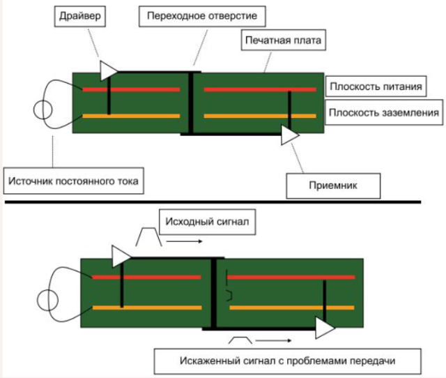
Signal distortion isn’t a significant issue for PCBs operating at low frequencies, but it can be a serious problem for high-speed, high-frequency (>50 MHz) devices . In high-frequency mode, both digital and analog aspects of the signal must be considered. When a signal travels from the driver to the receiver, it doesn’t remain unchanged; whatever was originally sent will be received with varying degrees of distortion (Figure 1).
Signal distortion during its passage across a board occurs due to factors such as impedance mismatch, reflections, crosstalk, crosstalk, ground bounce, and jitter. The designer must strive to minimize these factors to ensure that the original signal reaches its destination with distortion below the error threshold. Special attention must also be paid to signal quality and the management of its unwanted effects on the electronic circuit.
Why is it important to ensure signal integrity on a printed circuit board?
The main reason is that if there are signal integrity issues, the PCB will likely not function as specified in the design documentation. The most frustrating aspect is that errors can occur intermittently: sometimes the board will function as expected, sometimes not. For example, a board might work during prototyping but begin to fail during mass production; it might remain functional in lab conditions but fail in the field; it might work in older production batches but not in newer ones, etc. Differences in board performance under these conditions will be determined by whether the board has lost signal integrity or not.
Signal integrity is considered lost if:
- the signal is distorted, that is, its shape changes compared to the required one;
- unwanted electrical noise is superimposed on the signal, degrading the signal-to-noise ratio (S/N);
- the signal itself creates unwanted noise for other signals and circuits on the board.
The integrity of the signal is considered intact if:
- all signals on the printed circuit board are transmitted without distortion;
- the components and interconnections of the board are immune to extraneous electrical noise and electromagnetic interference (EMI) from other nearby electronic devices, either meeting or exceeding regulatory standards;
- The board does not generate, create, or emit EMI that affects the operation of other electronic circuits, cables, or devices connected to or in close proximity to this board (also in accordance with or exceeding regulatory standards).
Nine Factors Leading to Signal Integrity Issues on a Printed Circuit Board (PCB). In modern high-tech PCBs, fast signal rise times and high frequencies become issues that can lead to signal integrity issues if the board is not designed correctly (Figure 2). This article describes the factors that contribute to signal integrity issues on a PCB, divided into nine categories for ease of understanding.
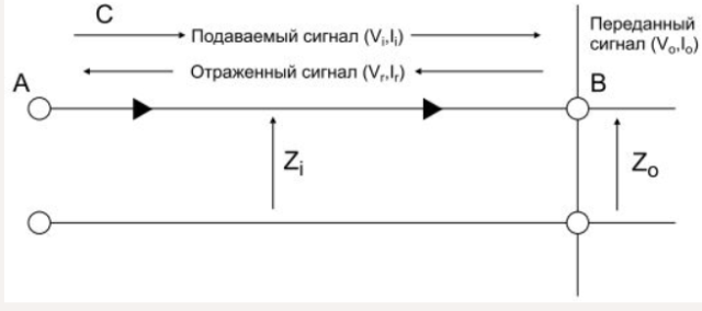
The quality of a signal in a circuit depends on the characteristics of the signal conductor and its return path. When a signal travels along a line and encounters changes or irregularities in line impedance, it is subject to reflections, which cause ringing and signal distortion. Furthermore, the faster the signal rise time, the greater the signal distortion caused by changes in uncontrolled line impedances. Minimizing signal distortion due to reflections can be achieved by reducing or eliminating line impedance changes. This requires:
- The signal lines and their return paths acted as uniform transmission lines with uniformly controlled impedances.
- Signal return paths in the form of homogeneous planes (layers) were placed near the signal layers.
- Controlled impedance signal lines have matched source/destination impedances similar to the characteristic impedance of the signal line by using proper PCB termination techniques.
Signal degradation due to other impedance discontinuities
As mentioned, if a signal encounters impedance discontinuities during propagation, it will experience reflections that cause ringing and distortion (Figure 3).
Signal degradation due to uncontrolled line impedances
Line impedance discontinuities occur at points that satisfy one or more of the following conditions:
- the signal encounters a via on its way;
- the signal is branched into two or more lines;
- there is a discontinuity on the signal return path, for example, a break in the layer at the point where the stubs are connected to the signal lines;
- the loops are connected to the signal lines;
- the signal line starts on the source side;
- the signal line is terminated at the receiver side;
- The signal and return paths are connected to the connector terminals.
Moreover, the faster the signal rise time, the greater its distortion caused by impedance inhomogeneities. Signal distortion due to line impedance inhomogeneities can be reduced in various ways:
- Minimizing the effects of discontinuities caused by vias and their stubs by using smaller microvias and HDI technologies.
- By reducing the length of conductor cables;
- By routing wires in a daisy chain topology rather than using multiple branches, which results in the signal being used in several places at once.
- Correct use of termination resistors on the source and receiver sides.
- By using differential signaling and densely packed differential pairs, which are inherently more resistant to inhomogeneities in the signal return planes (layers).
- Ensuring that at connectors where discontinuities occur, signal lines are as short as possible and signal return paths are as wide as possible.
Signal degradation due to propagation delay
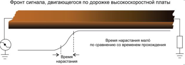
Signal transmission across a printed circuit board (PCB) from source to receiver is accompanied by a time delay. This delay is directly proportional to the length of the traces and inversely proportional to the signal propagation speed on the layers of the board. If the combined delays of clock and data signals are mismatched, they arrive at the receiving device at different points in time, creating signal skew. Excessive skew leads to timing imbalances and sampling errors. As operating frequencies and data rates increase, the detection time intervals shorten (the sampling frequency increases), reducing the permissible skew. This increases the system’s sensitivity to timing inconsistencies due to delays and increases the likelihood of errors. Skew in a group of signal lines can be minimized by matching the signal delays, which requires matching the trace lengths.
Signal degradation due to attenuation
Signals are attenuated as they propagate along printed circuit board (PCB) lines . This occurs due to losses caused by the resistance of the conductive paths—which increases at high frequencies due to the skin effect—and the dielectric loss factor (Df) of the dielectric material. Both types of losses increase with frequency, so high-frequency signal components will be subject to greater attenuation than low-frequency components. This narrows the signal bandwidth, which in turn leads to signal distortion due to increased rise time. Excessive signal rise time leads to data acquisition errors. Therefore, in situations where signal attenuation is a significant factor, it is essential to select the correct type of high-speed, low-loss material and ensure proper control of the conductor geometry to minimize losses.
Signal degradation due to crosstalk. Rapid changes in voltage or current on a signal line or return path layer can affect adjacent signal lines, causing unwanted signals called crosstalk and switching noise on adjacent signal lines (Figure 4).
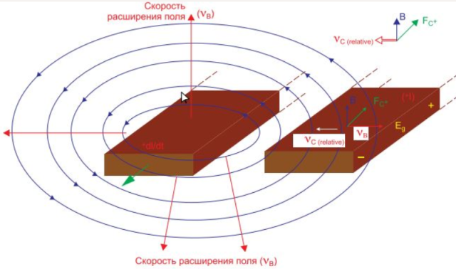
This type of coupling between adjacent signal lines occurs due to the mutual capacitance and mutual inductance between the conductors. This mutual capacitive and inductive coupling can be reduced by increasing the distance between the conductors. A rule of thumb is a ratio of 1:3, meaning the distance should be three times the conductor width (the 3W rule). It’s also important to remember that faster signals with shorter rise times create more crosstalk and transient interference.
Crosstalk and transient interference can be reduced by:
- increasing the distance between adjacent signal conductors;
- Ensuring the widest and most uniform signal return paths possible, similar to continuous layers. However, discontinuities in return paths should be avoided;
- using printed circuit board material with lower dielectric constant;
- the use of differential signaling and tightly spaced differential pairs, which are inherently more resistant to crosstalk.
Signal degradation due to power supply and grounding
Power and ground buses, or paths, have very low but measurable non-zero impedances. When output signals and internal gates switch states, currents through the buses, paths, and power and ground planes change, causing a voltage drop on these buses, which leads to a decrease in voltage at the power and ground pins of devices. The higher the frequency of such events, the shorter the signal transmission time, and the greater the number of lines switching states simultaneously, the greater the voltage drop on the power and ground buses. This reduces the noise immunity of signals and, if a certain threshold is exceeded, can cause device failure.
To reduce such effects, the power supply network must be designed to minimize the power supply system impedance by:
- The power and ground planes should be located as close to each other and to the PCB surface as possible. This will reduce the via inductance;
- Several low-inductance decoupling capacitors should be used between the power and ground rails, placing them as close as possible to the power and ground terminals of the devices;
- it is necessary to use components in packages with short leads;
- It should be taken into account that the use of thin high-capacity cores for the power and ground planes significantly increases the capacitance and reduces the impedance between the power and ground buses.
Signal degradation due to electromagnetic interference/electromagnetic compatibility
As frequency increases and signal rise times decrease, electromagnetic interference levels increase, increasing electromagnetic compatibility (EMI/EMC) requirements. Far-field radiation strength increases linearly with frequency for single-ended signal currents and quadratically with frequency for differential signal currents. Electromagnetic interference can also be reduced by shortening the current path.
Signal integrity issues due to via stub and trace stub
A via stub is the portion of a via not used for signal transmission. The via stub acts as a resonant circuit with a specific resonant frequency at which it accumulates maximum energy. If the signal has a significant component at or near this frequency, this component will be greatly attenuated due to the via stub’s energy requirement at its resonant frequency.
In the example shown in Figure 5, via section A is used to propagate the signal from conductor C1 on the outer layer to conductor Cn on the inner layer. However, via section B is redundant—thus, it is the via stub.
Long trace stubs can act as antennas, exacerbating EMC compliance issues. Conductor stubs can also create reflections, which negatively impact signal integrity. Pull-up or pull-down resistors in high-speed signal lines are commo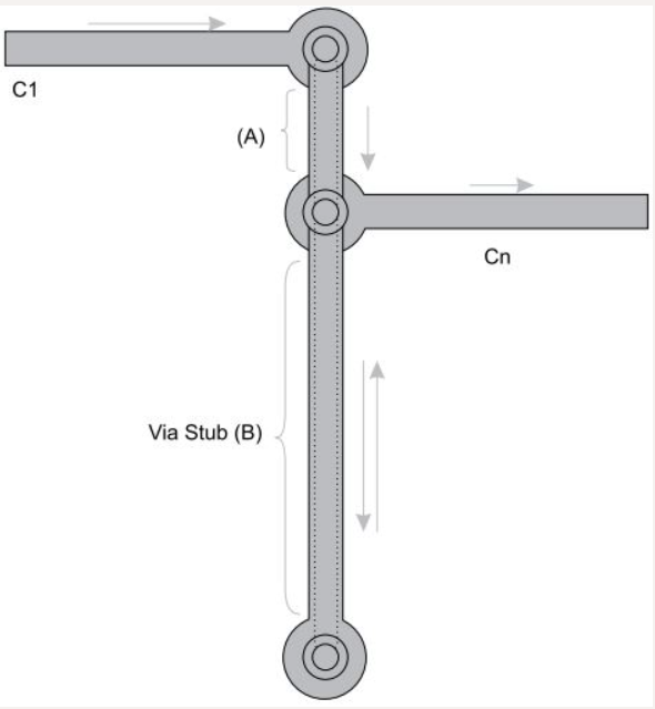
Signal integrity problems due to ground bounce
Due to excessive current draw, the circuit’s ground reference shifts from its original value. This occurs due to ground resistance and interconnections such as connecting wires and traces. Consequently, ground voltage levels will vary at different points. This phenomenon is known as ground bounce, as the ground voltage will vary depending on the current.
The following are effective methods for reducing ground bounce:
- use of decoupling capacitors connected to local ground;
- inclusion of series-connected current-limiting resistors;
- placement of decoupling capacitors near the terminals;
- organizing proper grounding.
Signal rise time is a critical parameter when dealing with signal integrity issues. To achieve the desired signal integrity level, attention should be paid to:
- impedance control;
- signal attenuation;
- ground potential surges;
- signal propagation delays;
- electromagnetic interference/compatibility (EMI/EMC).
Signal integrity measures must be implemented at the printed circuit board (PCB) design stage . Otherwise, the designer will have to repeatedly redesign the entire design to eliminate the causes of signal integrity issues that lead to board malfunctions.
