// Multilayer PCB ManufacturingMultilayer PCB with Blind/Buried Via & Mixed Material
KKPCB specializes in the manufacturing of high-quality multilayer printed circuit boards designed for advanced and high-reliability electronic applications. With state-of-the-art equipment and precise process control, we are capable of producing complex multilayer PCBs featuring blind and buried vias, mixed materials, and fine traces. Our experienced engineering team provides full DFM support to ensure manufacturing accuracy, signal integrity, and cost efficiency. Trusted by customers worldwide, KKPCB continues to deliver multilayer PCB solutions that combine innovation, performance, and reliability.
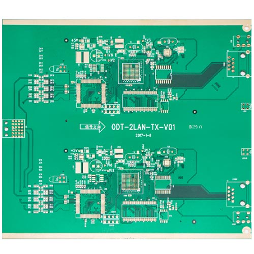
8-Layer Medical Device PCB
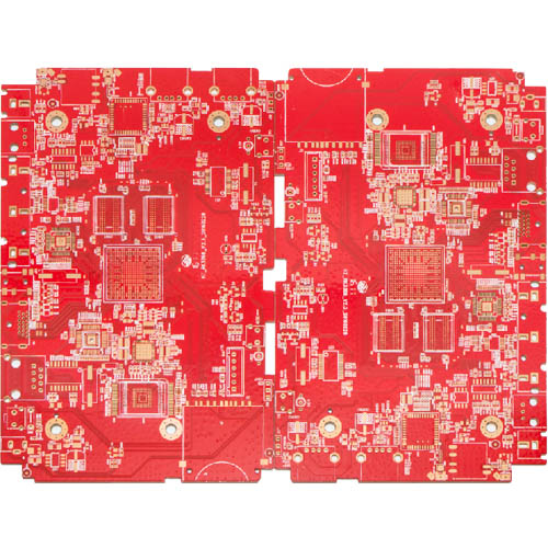
High-Tg Multilayer PCB
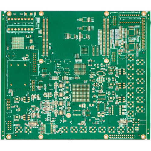
HDI Multilayer PCB
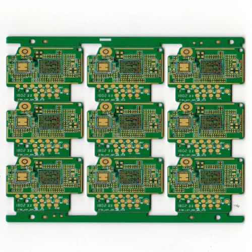
6-Layer PCB for Security Control Systems
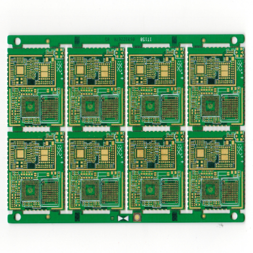
8-Layer PCB for Industrial Control Systems
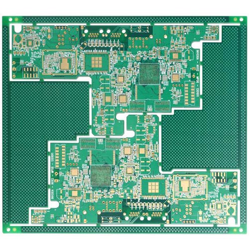
6-Layer Industrial Control PCB
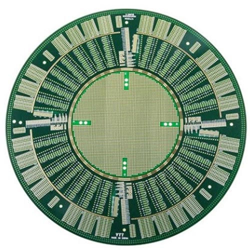
IC Chip Test PCB
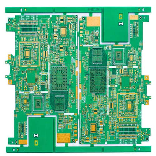
12-Layer PCB with Copper-Filled Vias
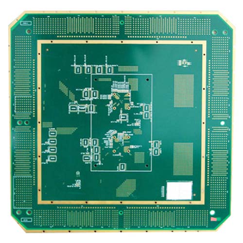
ST115G Multilayer PCB
What is multilayer PCB?
Multilayer PCB board refers to a PCB that has more than three conductive pattern layers and is laminated with insulating materials between them. With the development of electronic technology to high-speed, multi-function, large capacity, and portable low-consumption direction, the application of multi-layer PCB is more and more widely, and its layer number and density are also higher and higher, and the corresponding structure is also increasingly complex. The production of multilayer PCB has become the most important part of the whole PCB industry. At present, the average number of layers of KKPCB has reached 8-20 layers, can up to 64 layers, which has reached a high level in terms of inner layer manufacturing ability and laminating ability. The emergence of multi-layer board technology is a major development of the PCB industry, which makes the whole PCB technology advance by leaps and bounds.

KKPCB is very good at multilayer PCB fabrication and prototyping. The manufacturing process of ordinary multilayer PCB is mainly based on lamination technology. Multi-layer lamination is an important process in PCB manufacturing. KKPCB has been producing multilayer PCBs for over 20 years. Over the years, we have seen all types of multilayer constructions from various industries, answered all types of multilayer questions, and solved all types of problems with multilayer PCBs.
Multilayer PCB Lamination

1. The thickness of the core board should be selected according to the total thickness requirements of the multilayer board. The thickness of the core board should be consistent and the deviation is small.
2. There should be a certain distance between the overall dimension of the core board and the effects unit, that is, the distance from the effective unit to the edge of the board should be on the premise of not wasting materials try to keep more space.
3. Design of positioning hole. In order to reduce the deviation between layers, attention should be paid to the design of positioning holes in multi-layer boards: 4-layer multilayer only needs to be designed more than 3 positioning holes can be used for drilling. For multi-layer boards with more than 6 layers, in addition to designing positioning holes for drilling, it is also necessary to design more than 5 overlapping positioning rivet holes and more than 5 positioning holes for the tool plate for rivets.
4. The inner core board shall be free from the open, short, open circuit, oxidation, clean board surface, and no residual film.
5. Meet the requirements of PCB users, select the appropriate PP and copper foil configuration. For 4-ply laminates, 7628, 3313 or 7628 + 1080, 7628 + 2116 can be used etc. 1080 or 2116 is the main choice of PP for multilayer boards with more than 6 layers, and 7628 is mainly used to increase the thickness of the dielectric layer. At the same time, PP requires symmetrical placement to ensure mirror effect and prevent plate bending.
6. Inner core board pretreatment process. The treatment process of the inner layer core board includes the black oxidation process and browning treatment process. The oxidation treatment process is to form a black oxide film on the inner copper foil, the thickness of the black oxide film is 0.25-4.50mg/cm2. The browning process (horizontal browning) is to form an organic film on the inner copper foil.
The functions of the inner laminate treatment process are as follows:
a. Increasing the surface ratio of inner copper foil and resin can enhance the adhesion between them.
b. The effective wettability of the melt resin to copper foil is increased so that the flowing resin has sufficient ability to penetrate into the oxide film and show a strong grip after curing.
c. It can prevent the decomposition of dicyandiamide in liquid resin at high temperatures and influence on the copper surface.
d. It can improve the acid resistance and prevent the PINK ring in the wet process.
7. The organic matching of lamination parameters, the control of multi-layer board lamination parameters mainly refers to the organic matching of lamination “temperature, pressure, and time”. How to determine the lamination temperature, pressure, and time software parameters is the key technology for multilayer laminate processing.
Materials for making multilayer PCB
1. Copper Foil
Function: Forms the conductive patterns on the PCB.
Description: Copper foil is the essential material for the PCB’s conductive layers, providing the electrical pathways necessary for signal transmission and overall board performance.
2. Core Board
Function: Serves as the structural framework of the PCB.
Description: A double-sided copper-clad laminate that acts as the backbone of the circuit board. Core boards provide mechanical stability and serve as the foundation for double-sided or multilayer PCB production.
3. Prepreg
Function: Acts as both adhesive and insulator between core boards in multilayer PCBs.
Description: Prepreg is an indispensable material in multilayer PCB manufacturing. It bonds core boards together while providing electrical insulation. During lamination, prepreg ensures strong interlayer adhesion, preventing short circuits and maintaining structural integrity.
| Material Name | Material Type | Base Thickness (μm) |
|---|---|---|
| FR4 | 7628 | 193 |
| 1506 | 150 | |
| 2116 | 122 | |
| 3313 | 99 | |
| 1080 | 74 | |
| 106 | 60 |
Difference Between Single-Layer and Multilayer PCBs
Compared with single-layer or double-layer PCBs, multilayer PCBs offer significantly improved electromagnetic compatibility (EMC) and enhanced electrical performance.
For example, in a four-layer PCB, the inner layers are often designated as a power plane and a ground plane, which provides the following benefits:
-
Reduced Inductance: The inductance of power and ground traces is greatly reduced, lowering noise voltage.
-
High-Frequency Decoupling: The power and ground planes form a large distributed capacitor, providing excellent high-frequency decoupling for the power supply and reducing power line noise.
-
Minimized Signal Loops: Independent power and ground planes help minimize the loop area for all signal paths, improving signal integrity.
-
Industry Trend Toward Miniaturization: Modern PCBs are trending toward smaller sizes, thinner layers, smaller vias, higher layer counts, and finer trace widths and spacing—making multilayer designs essential.
-
Support for Advanced Electronics: Many high-precision and high-tech electronic devices require multilayer PCBs to achieve their functions. Standard double-sided boards cannot meet these advanced requirements.
Conclusion: Multilayer PCBs are indispensable for modern electronics, providing superior noise control, signal integrity, and support for compact, high-density circuit designs.
Types of Multilayer PCBs
1. Classification by Application
-
Consumer Electronics PCBs: Used in TVs, electronic toys, smartphones, and other consumer devices.
-
Industrial PCBs: Used in computers, instrumentation, automation systems, and other industrial equipment.
-
Military & Aerospace PCBs: Designed for high-reliability applications in defense and aerospace, often meeting strict environmental and performance standards.
2. Classification by Flexibility / Hardness
-
Rigid PCBs: Solid, inflexible boards for traditional electronic devices.
-
Flexible PCBs (Flex): Can bend or fold to fit compact spaces or dynamic applications.
-
Rigid-Flex PCBs: Combination of rigid and flexible sections, ideal for high-density, complex assemblies.
3. Classification by Via / Hole Technology
-
Buried Via PCBs: Vias that connect inner layers without reaching the outer layers.
-
Blind Via PCBs: Vias that connect outer layers to inner layers without going through the entire board.
-
Blind-Buried / HDI PCBs: High-Density Interconnect PCBs combining blind and buried vias for miniaturized, high-performance circuits.
-
Through-Hole PCBs: Vias that pass through all layers of the board, commonly used for mounting components.
4. Classification by Substrate Material
-
FR4 (Glass Cloth) PCBs: Standard rigid boards based on glass-epoxy material.
-
Ceramic Substrate PCBs: Used for high-frequency, high-temperature, or high-power applications.
-
Metal-Core PCBs (MCPCBs): Offer excellent heat dissipation for LED and power applications.
Application of Multilayer PCB
As mentioned above, multilayer PCB can be used in civil, industrial, and military fields. Multilayer PCB can be used for any purpose.
For many industries, multilayer PCB has become the first choice for various applications. This preference is largely due to the continuous promotion of mobility and functionality by all technologies. Multilayer PCB is a reasonable step in this process, which can reduce the size and realize more functions. As a result, they have become quite common, including:
- Consumer electronics: consumer electronics is a broad term, such as smartphones and microwave ovens. Each of these consumer electronics products contains PCB, but more and more of them use multilayer PCB instead of standard single-layer PCB, which is used to increase function and reduce size.
- Computer electronics: everything from the server to the motherboard uses multilayer PCBs, mainly because of their space-saving and high functionality. For these applications, performance is one of the most basic characteristics of PCB.
- Telecommunications: telecommunications equipment typically uses multilayer PCBs in a variety of general applications, such as signal transmission, GPS, and satellite applications. The main reason is its durability and functionality.
- Industrial: Multilayer PCB has become popular in several industrial applications, the most notable of which is industrial control. From industrial computers to control systems, multilayer PCBs are used to run machines throughout manufacturing and industrial applications, contributing to their durability and small size.
- Medical devices: electronic products are becoming an increasingly important part of the healthcare industry, playing a role in every corner of the industry, from treatment to diagnosis. Compared with single-layer substitutes, multilayer PCB is particularly popular in the medical industry because of its small size, lightweight and powerful functions. These advantages make multilayer PCB used in modern X-ray equipment, cardiac monitor, CAT scanning equipment, and medical test equipment.
- Military and national defense: multilayer PCBs are favored in terms of durability, functionality, and low weight, and are very useful in high-speed circuits, which are getting more and more attention in military applications. As the defense industry moves towards highly compact engineering, they are also favored, as smaller multi-layer PCBs leave more space for other components to perform their existing functions.
- Automobile: in the modern automobile, the automobile is more and more dependent on electronic components, especially with the rise of an electric vehicles. From GPS and onboard computers to headlight switches and engine sensors controlled by electronic devices, using the right type of components is becoming increasingly important in vehicle design. Multilayer PCB has high function and relative heat resistance, so it is very suitable for the interior environment of automobiles.
- Aerospace: like cars, jets, and KKPCB, they rely heavily on modern electronics, all of which have to be very precise. From the computer used on the ground to the computer used in the cockpit, the application of aerospace PCB must be reliable. In this case, multilayer PCB is the ideal solution, with enough protection layer to keep heat and external stress from damaging the connection, and the ability to be made of flexible materials. Their higher quality and functionality also contribute to this utility in the aerospace industry, as aerospace companies prefer to use the best materials to ensure the safety of personnel and equipment.
- There are more! Multilayer PCB is used in a variety of other industries, including the science and research industry, even household appliances and safety. All devices, from alarm systems and optical fiber sensors to atomic accelerators and weather analysis equipment, use multilayer PCBs, making full use of the space and weight saved by this PCB format.
KKPCB is widely known as a professional PCB supplier in the electronic manufacturing industry. We have years of experience in the multilayer PCB, HDI PCB segments. KKPCB further expands its range of products including rigid, rigid-flex, HDI, any layer, Flex, large-size, embedded, RF, LED, backplane, the metal substrate, a ceramic substrate, IC structure, high-frequency, heavy copper. High quality and high reliability.
Multilayer PCB Design Guide
Designing a multilayer PCB requires careful planning and attention to detail to ensure high performance, signal integrity, and long-term reliability. Below are the key considerations for successful multilayer PCB design.
1. Layer Stackup Planning
- The stackup defines how signal, power, and ground layers are arranged.
- A well-planned stackup reduces crosstalk, electromagnetic interference (EMI), and noise, while improving signal integrity.
- Poor stackup or improper layer configuration can lead to timing glitches, signal distortion, and intermittent operation.
2. Material Selection
- Choosing the right substrate and copper foil is critical.
- Materials with appropriate dielectric constant, thermal performance, and mechanical stability ensure reliable signal transmission and robust operation.
- Incorrect material choice can increase emission, reduce performance, and make the PCB susceptible to environmental noise.
3. Signal Integrity & EMI Control
- Proper placement of ground and power planes minimizes loop areas and reduces inductance.
- High-speed signals require controlled impedance traces and careful routing to reduce crosstalk and reflection.
- Multilayer boards allow dedicated planes for power and ground, acting as distributed capacitors to improve high-frequency decoupling.
4. Design Best Practices
- Minimize via count and keep signal paths as short and direct as possible.
- Maintain consistent layer symmetry to prevent warping and ensure mechanical stability.
- Separate analog and digital signals when possible to reduce interference.
- Plan for thermal management, especially in high-power or high-density applications.
Multilayer PCB Design Guide
Designing a multilayer PCB requires careful planning to ensure high performance, signal integrity, and long-term reliability. Proper design reduces noise, electromagnetic interference (EMI), and crosstalk while optimizing space and functionality.
1. Layer Stackup Planning
-
The stackup defines the arrangement of signal, power, and ground layers.
-
A well-planned stackup reduces crosstalk, EMI, and noise, and improves signal integrity.
-
Poor stackup or improper layer configuration can lead to timing glitches, signal distortion, and intermittent operation.
Stack Design Guidelines:
-
Ground Plane Placement: Place a ground plane directly below the component layer to provide shielding and a reference for surface wiring.
-
Signal Layer Adjacency: All signal layers should be adjacent to a ground plane whenever possible.
-
Avoid Back-to-Back Signal Layers: Prevent placing two signal layers directly adjacent to each other.
-
Power-Ground Pairing: Place the main power plane as close as possible to its corresponding ground plane to reduce inductance and noise.
-
Symmetry: Maintain symmetry in dielectric layer thickness, copper foil thickness, and layer geometry to prevent warping and mechanical stress.
-
Balanced Distribution: Ensure the distribution of large copper planes and circuit layers is symmetrical for electrical and mechanical stability.
Effectiveness:
-
Compared to double-sided PCBs, a properly designed four-layer PCB can reduce radiation by approximately 15 dB.
-
Proper stackup provides a low-inductance distribution network and improves high-speed performance.
2. Material Selection
-
Choose the right substrate and copper foil for dielectric constant, thermal performance, and mechanical stability.
-
Incorrect material selection can increase EMI, reduce signal integrity, and make the PCB vulnerable to external noise.
3. Signal Integrity & EMI Control
-
Proper placement of ground and power planes minimizes loop areas and inductance.
-
High-speed signals require controlled impedance traces and careful routing to reduce crosstalk and reflection.
-
Multilayer boards allow dedicated planes for power and ground, acting as distributed capacitors for high-frequency decoupling.
4. Design Best Practices
-
Minimize via count and keep signal paths short and direct.
-
Separate analog and digital signals where possible.
-
Plan for thermal management in high-power or dense layouts.
-
Maintain layer symmetry to prevent mechanical stress and warping.
Let’s take a look at the most common multilayer PCB Lamination
4-Layer PCB Lamination
Lamination is a critical process in multilayer PCB manufacturing, where multiple layers of copper and dielectric materials are bonded together under heat and pressure to form a solid, reliable PCB. Proper lamination ensures mechanical stability, signal integrity, and consistent electrical performance.
Typical 4-Layer PCB Structure
-
Top Layer (Signal Layer): Component wiring and signal traces.
-
Inner Layer 1 (Ground Plane): Provides shielding and a reference plane for signals.
-
Inner Layer 2 (Power Plane): Distributes power efficiently and reduces noise.
-
Bottom Layer (Signal Layer): Additional routing for signals and components.
Key Advantages
-
Improved Electromagnetic Compatibility (EMC): Reduces radiation and crosstalk.
-
Low Inductance Power Distribution: Enhances high-frequency performance and signal integrity.
-
Compact Design: Supports smaller size and higher functionality for modern electronics.
-
Mechanical Stability: Symmetrical lamination reduces warping and ensures long-term reliability.
A well-designed 4-layer lamination is essential for high-performance applications across consumer electronics, industrial control, medical devices, automotive, aerospace, and military sectors.

4 Layer PCB stack
Four layers of PCB are usually seen stacked evenly. That is, four evenly spaced layers with the plane at the center. While this does make the board symmetrical, it does not help EMC.
In addition, another common mistake is to make the plane tightly coupled to the large dielectric layer and plane between the center and the signal. This certainly produces good interplane capacitance, but it also doesn’t help signal integrity, crosstalk or EMC – that’s why we chose to use 4-layer PCBs on two layers.
To improve the EMC performance of the capacitor, it is better to put the signal layer as close as possible to the plane (< 10 mil), and use a large core (~ 40 mil) between the power supply and the ground plane to maintain the overall substrate thickness 62 mil. Close tracking of planar coupling will reduce crosstalk between traces and allow us to keep impedance at an acceptable value.
6 Layer PCB stack
The six-layer PCB board is basically a four-layer board, adding two additional signal layers between the planes. This greatly improves EMI because it provides two buried layers for high-speed signals and two surface layers for routing low-speed signals. The signal layer should be placed very close to the adjacent plane and the plate thickness (62 mil) should be composed of a thicker central core. There is always a trade-off between trace impedance, trace width and prepreg/core thickness. Differential pairs are becoming more and more common in high-speed design. Noise is reduced by using differential mode signals.

6 Layer PCB stack & 8 Layer PCB stack
To improve EMC performance, add two more planes in the six stack. It is recommended not to have more than two adjacent signal layers between the planes as this creates impedance discontinuities (signal layer impedance difference of ~ 20 Ohm) and increases crosstalk between these signal layers.
In the following case, two plane layers are added to the center of the substrate. This allows tight coupling between the central planes and isolates each signal plane, thereby reducing coupling and significantly increasing crosstalk. This configuration is usually used for high-speed signals in DDR2 and DDR3 designs where crosstalk due to tight wiring is a problem.
10 Layer PCB stack
When six wiring layers and four planes are required, ten layer boards should be used – and EMC deserves attention.

A typical 10 layer overlay is shown above. This superposition is ideal because of the tight coupling of the signal and returns plane, the shielding of the high-speed signal layer, the presence of multiple ground planes, and the symmetry of tightly coupled power/ground at the center of the circuit board. High-speed signals are usually routed on signal layers buried between planes (in this case, layers 3-4 and 7-8). However, care should be taken to route these signals correctly. Other, avoid coupling (crosstalk) between adjacent layers.
12 layer PCB stack
12 layers are the maximum number of layers that can be easily made in 62mil thick PCB. Occasionally you’ll see 14 to 16 layers of boards made into 62mil thick boards, but the number of manufacturers that make them is limited to those who can make HDI boards. The above twelve stacked layers provide shielding on six inner layers.

12 Layer PCB stack &14 Layer PCB stack
When eight routing (signal) layers are required, a special critical shield is required to use the 14 layer overlay below. Layers 6 and 9 provide isolation for sensitive signals and 3, 4 and 11, 12 provide shielding for high-speed signals.

14 Layer PCB stack & 16 Layer PCB stack
16 Layer PCB provides ten layers of wiring, which are usually used in extremely dense designs. Typically, you will see a 16 layer PCB where the routing technology used in EDA applications cannot route the design to completion. “If it doesn’t route – just continue adding layers. “. Although this is a common saying, it is not a good practice.
If the board cannot complete the route, then there may be many reasons. Bad placement is often. Open the routing channels, reduce the number of crosses in the rat network, place vias on the 25 mil grid to allow routing and help routers as much as possible.

16 Layer PCB stack
The number of layers that can be manufactured is not actually limited to Multilayer PCB (please check the manufacturer’s function first). Of course, as the number of layers increases, the PCB thickness increases to accommodate the minimum thickness of the material used. The aspect ratio (board thickness and minimum hole size) must also be considered. Generally speaking, the thickness of 100 Mil material is 10:1. For example, a 200 mil thick substrate has a minimum hole size of 20 mils.
Determine the number of layers
The technical rule is based on the minimum spacing of SMT components used, which is basically the maximum routing, clearance and through-hole allowed while minimizing PCB manufacturing costs. Complex high-speed designs using a ball grid array (BGA) usually require 4 / 4 mil (routing/gap) and 20 / 8 mil (PAD/hole) via technology. However, if you can, use smaller sizes, which will reduce costs and increase manufacturing output.
Once these rules are established, the required characteristic impedance (Zo) and differential impedance required stack (Zdiff) are calculated according to the component datasheet. Typically, 50 ohm Zo and 100-ohm Zdiff are used. Keep in mind that lower impedances increase the di / dt and significantly increase the absorbed current (which is detrimental to the PDN), and higher impedances generate more EMI and make the design more susceptible to external influences. Therefore, a good Zo range is 50-60 ohm.
The total number of layers required for a given design depends on the complexity of the design. Factors include the number of signaling networks that must break through from BGA; the number of power supplies required by BGA; component density and package type.
Experienced designers will know about it after a while, but checking that there are enough layers is a good way to automatically adjust the board. If not adjusted, the router needs to complete at least 85% of the routing to indicate that the selected stack is routable. You may need to reevaluate the placement several times for the best results.
// Frequently Asked Questions (FAQ)Multilayer PCB FAQ
A multilayer PCB (Printed Circuit Board) is composed of three or more layers of conductive material (such as copper foil) and insulating material (such as FR4) stacked alternately. Its structure typically includes:
- Outer Layers: The top and bottom conductive layers used for placing components and connecting wires.
- Inner Layers: The middle conductive layers used for internal connections in complex circuits.
- Insulating Layers: The insulating materials between conductive layers used for electrical isolation and mechanical support.
Advantages of Multilayer PCBs
-
- Higher Design Density: The multilayer structure allows for more wiring and component integration, suitable for complex circuit designs.
- Better Electrical Performance: Multilayer boards can reduce signal transmission paths, improve signal integrity, and reduce electromagnetic interference (EMI).
- Smaller Size: Multilayer design can reduce the overall size of the PCB, suitable for compact devices.
- Enhanced Reliability: The multilayer structure can achieve higher mechanical strength and reliability.
Multilayer PCBs are widely used in the following fields:
- Consumer Electronics: Such as smartphones, tablets, laptops, etc.
- Communication Equipment: Such as routers, switches, base stations, etc.
- Automotive Electronics: Such as onboard computers, navigation systems, sensor modules, etc.
- Industrial Control: Such as PLCs, sensors, control systems, etc.
- Medical Devices: Such as MRI, CT scanners, monitors, etc.
Multilayer PCBs (Printed Circuit Boards) differ from regular (single-layer or double-layer) PCBs in several key aspects, including their structure, complexity, capabilities, and applications. Here are the main differences:
Structural Differences
- Number of Layers:
- Single-layer PCB: Has only one layer of conductive material (copper) on one side of the substrate.
- Double-layer PCB: Has conductive layers on both sides of the substrate, allowing for more complex circuits.
- Multilayer PCB: Consists of three or more conductive layers separated by insulating materials. The layers are interconnected by vias (through-holes or blind/buried vias).
- Interconnections:
- Single-layer and Double-layer PCBs: Interconnections are limited to the top and bottom layers.
- Multilayer PCBs: Allow for complex interconnections across multiple internal layers, enabling more sophisticated designs.
Complexity and Design
- Design Complexity:
- Single-layer PCBs: Suitable for simple, low-density circuits.
- Double-layer PCBs: Can handle moderate complexity, offering more routing options than single-layer.
- Multilayer PCBs: Ideal for highly complex designs with dense circuitry, multiple signal layers, power planes, and ground planes.
- Signal Integrity:
- Single-layer and Double-layer PCBs: May struggle with signal integrity in high-speed applications due to limited routing options.
- Multilayer PCBs: Better signal integrity and reduced electromagnetic interference (EMI) due to dedicated power and ground planes, and controlled impedance routing.
Capabilities
- Electrical Performance:
- Single-layer and Double-layer PCBs: Sufficient for low to moderate performance requirements.
- Multilayer PCBs: Enhanced electrical performance, suitable for high-speed, high-frequency applications, and complex signal processing.
- Component Density:
- Single-layer and Double-layer PCBs: Limited component density due to fewer routing layers.
- Multilayer PCBs: Higher component density, allowing for more compact designs and greater functionality.
Applications
- Single-layer PCBs: Used in simple, low-cost electronics like calculators, power supplies, and household appliances.
- Double-layer PCBs: Common in moderately complex devices like lighting systems, amplifiers, and some consumer electronics.
- Multilayer PCBs: Essential for advanced electronics, including smartphones, computers, high-speed communication devices, automotive systems, industrial control equipment, and medical devices.
Manufacturing Considerations
- Cost:
- Single-layer PCBs: Cheapest to manufacture due to their simplicity.
- Double-layer PCBs: Slightly more expensive than single-layer due to additional processing steps.
- Multilayer PCBs: Most expensive due to their complexity, multiple layers, and additional manufacturing processes.
- Manufacturing Process:
- Single-layer and Double-layer PCBs: Simpler manufacturing processes with fewer steps.
- Multilayer PCBs: More complex manufacturing involving layer alignment, lamination, drilling, and via plating.
In summary, multilayer PCBs provide greater design flexibility, higher performance, and the ability to handle more complex and compact designs compared to single-layer and double-layer PCBs, making them suitable for advanced and high-demand applications.
The production of multilayer PCBs relies on various sheet materials for substrates and dielectric layers, chosen based on performance, thermal requirements, mechanical strength, and application needs. Substrate materials commonly include FR4, a woven fiberglass cloth with epoxy resin, offering a balance of mechanical strength, electrical insulation, flame retardance, and cost-effectiveness; Polyimide, used in high-temperature and flexible PCBs for its excellent thermal and mechanical properties; PTFE, ideal for high-frequency RF and microwave circuits due to its low dielectric constant and minimal signal loss; and CEM-1/CEM-3, cost-effective composite epoxy materials suitable for less demanding applications.
Dielectric materials include prepreg, fiberglass impregnated with resin, which acts as both an adhesive and an insulating layer between conductive layers, and core sheets, thin rigid dielectric layers (like FR4) laminated with copper foil to provide structural support. Advanced dielectric materials include Rogers laminates, BT epoxy (Bismaleimide-Triazine), and Teflon (PTFE), offering superior high-frequency performance, thermal stability, and electrical properties for demanding applications.
Specialized materials are also used in multilayer PCB manufacturing, such as ceramic substrates for high-power or high-temperature applications, and metal core PCBs (MCPCBs) with aluminum or copper cores, providing excellent heat dissipation and mechanical stability, often used in LED lighting and power electronics. Selecting the appropriate sheet materials is critical to achieving the desired electrical, thermal, and mechanical performance of multilayer PCBs.
Testing multilayer PCBs is essential to ensure their reliability and proper functionality. Common testing methods include visual inspection, both manual and automated (AOI), to detect visible defects such as misaligned components, solder bridges, or bad joints. Electrical testing ensures correct connectivity and isolation, using continuity tests, isolation tests, in-circuit testing (ICT), and flying probe testing for prototypes or small batches. Functional tests simulate real-world conditions to verify PCB operation, while X-ray inspection evaluates internal layers, solder joints, and buried components for hidden defects. Thermal imaging detects hot spots and overheating issues, and impedance testing ensures controlled impedance traces meet design specifications using tools like Time Domain Reflectometers (TDR). Solderability testing checks the quality of solderable surfaces, and environmental stress testing, including thermal cycling, humidity, and vibration tests, evaluates performance under extreme conditions. By combining multiple testing methods, manufacturers can comprehensively assess PCB quality, identify potential issues early, and ensure optimal performance in the final application.
The production of multilayer PCBs (Printed Circuit Boards) involves a series of sequential steps, each critical for ensuring the quality, reliability, and functionality of the final product. The process begins with design preparation, including reviewing customer-provided files, verifying manufacturability, and panelization for efficient production. Next, material preparation involves selecting appropriate substrates (e.g., FR4, polyimide, PTFE), preparing copper foils, and cutting prepreg and core materials to required dimensions. During layer stack-up, the layers of copper and prepreg are aligned and bonded under heat and pressure to form the multilayer structure.
Drilling and plating follow, where precise CNC drilling creates through-holes, blind vias, and buried vias, and conductive plating ensures electrical connections between layers. Imaging and etching define circuit patterns on both inner and outer layers using laser direct imaging (LDI) and chemical etching. A solder mask is then applied and cured to protect copper surfaces while leaving pads and vias exposed, followed by silkscreen printing for component identifiers, markings, and logos.
During final finishing, individual PCBs are routed and profiled, and electrical testing verifies continuity, isolation, and impedance. Rigorous inspection and quality control, including manual visual checks and automated optical inspection (AOI), ensure defect-free PCBs. Finally, the boards are packaged and shipped securely to customers or assembly facilities. Throughout the process, advanced manufacturing technologies, precise process control, and comprehensive quality assurance ensure that each multilayer PCB meets design specifications, industry standards, and customer expectations, enabling reliable performance across a wide range of electronic applications.
Selecting a professional multilayer PCB manufacturer is crucial to ensure the quality, reliability, and timely delivery of your PCB boards. Key factors to consider include experience and reputation, as a manufacturer with a proven track record and positive customer feedback is more likely to handle complex designs successfully. Evaluate their capabilities and technology, ensuring they specialize in multilayer PCBs and use advanced equipment to improve manufacturing quality and efficiency. Quality assurance and certifications are essential; look for adherence to standards such as ISO 9001, ISO 13485, or AS9100, along with robust testing and inspection protocols.
Consider design and engineering support, including services to optimize manufacturability, troubleshoot design issues, and provide expert guidance. Assess their prototyping and production capabilities, ensuring they can handle both small-batch prototypes and large-scale production. Cost and pricing should be transparent, balancing affordability with the quality and reliability offered. Examine supply chain management, including reliable sourcing of materials and components, as well as clear lead times to meet project timelines. Strong customer support and communication are vital for responsiveness and proactive problem-solving throughout production. Additionally, location and logistics affect shipping efficiency and delivery times, while adherence to environmental and ethical practices ensures responsible manufacturing.
By carefully evaluating these factors, you can select a professional multilayer PCB manufacturer that meets your technical requirements, aligns with your project goals, and ensures successful deployment of your PCB designs.
