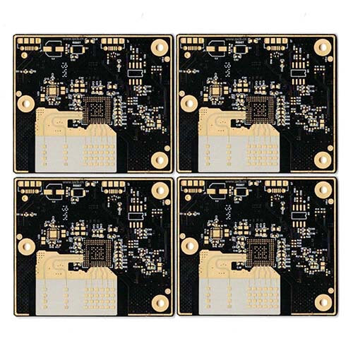
// High-Frequency PCB Product ShowcaseHigh-Frequency PCB, RF PCB & Microwave PCB Products
KKPCB is a leading manufacturer of high-frequency PCBs, offering a full range of rigid, flexible, rigid-flex, HDI, RF, microwave, multilayer, hybrid, and ATE high-frequency boards for demanding applications such as 5G, telecommunications, radar, satellite, automotive radar, IoT, and high-speed data communication. Using advanced materials like Rogers, Taconic, Arlon, Isola, Teflon, Dupont, and Shengyi, our PCBs provide low dielectric constant (Dk), low dissipation factor (Df), low thermal expansion (CTE), precise impedance control, and minimal signal loss. With rigorous quality control, advanced manufacturing processes, and engineering expertise, KKPCB delivers customized, reliable, and high-performance high-frequency PCB solutions that meet the most demanding project requirements.

Hybrid High-Frequency PCB RO4350B

Taconic High-Frequency PCB

Rogers RO3006 PCB
What is a High-Frequency PCB?
High-frequency PCB board or RF microwave PCB refers to the special circuit board with high electromagnetic frequency, which is used for high frequency (frequency greater than 300MHz or wavelength less than 1m). Generally speaking, a high-frequency board can be defined as a circuit board with a frequency above 1GHz. Substrate materials need to have excellent electrical properties and good chemical stability. With the increase of power signal frequency, the loss requirement on the substrate is very small, so the importance of high-frequency material is highlighted.
High-frequency PCB board with induction heating technology has been widely used in the communication industry, network technology, and high-speed information processing system, which meets the requirements of many high-precision parameter instruments. A reliable high-frequency circuit board, in the actual production, provides great help.

High-frequency PCB is widely used in RF and Microwave PCB. High-frequency PCB materials are different from conventional FR4 materials. Most of them use PTFE &Teflon materials. Good electrical properties and low signal loss are the basis.
High-frequency PCB needs special materials to realize the high-frequency signal provided by this type of printed circuit board. Many PCB designers choose Rogers dielectric material because of its lower dielectric and signal loss, lower circuit manufacturing cost, and more suitable for rapid turnover prototype application.In addition to selecting the right PCB material and determining the correct Er value, the designer should also consider the conductor width and spacing, substrate constant, and other parameters. The highest level of process control must be used to specify and implement these parameters precisely.KKPCB is an experienced full-service high-frequency PCB manufacturer, which can provide reliable and excellent high-frequency PCB fabrication services. Evaluate your requirements according to your design, rich variety of high-frequency materials, mature high-frequency PCB manufacturing experience.
KKPCB is an experienced full-service high-frequency PCB manufacturer, which can provide reliable and excellent high-frequency PCB fabrication services. Evaluate your requirements according to your design, mature high-frequency PCB manufacturing experience. Professional production experience for high frequency circuit boards used in power divider, coupling and device, circuit builder, amplifier, dry release, base station 3G antenna. Company year-round stocks domestic and imported high-frequency material (F4B Rogers, TACO, NC, ARLON, TP-2) dielectric constant 22106, etc. Can provide fast sample service and mass production in time to meet your diverse, multi-variety needs.
What are the advantages of high-frequency PCB?
High Efficiency
High-frequency Printed Circuit Boards with a low dielectric constant exhibit minimal signal loss. Combined with advanced induction heating technology, they achieve precise target heating with exceptional efficiency. In addition to high performance, these boards are environmentally friendly, aligning with the sustainable development trends of modern society.
Fast Signal Transmission
The signal transmission speed is inversely proportional to the square root of the dielectric constant, meaning lower dielectric constants result in faster signal propagation. High-frequency PCBs use specialized materials that not only ensure a small dielectric constant but also maintain stable operation, which is critical for high-speed and reliable signal transmission.
Precise and Flexible Regulation
High-frequency circuit boards are widely applied in precision heating of metal components across various industries. They can deliver localized or deep-level heating with exceptional accuracy, allowing both surface and internal component treatment, as well as focused or dispersed energy application, providing unmatched control and adaptability.
Superior Environmental Tolerance
The performance of conventional PCBs can be compromised by humidity and adverse environmental conditions. High-frequency PCBs made from low water absorption materials can withstand these challenges. In addition, they offer chemical corrosion resistance, moisture resistance, high-temperature stability, and excellent peel strength, ensuring consistent, reliable performance in demanding environments.
Processing characteristics of high-frequency PCB
High-frequency Printed Circuit Boards (PCBs) have strict fabrication requirements due to their specialized materials and high-performance applications:
- Precise Impedance Control: Line width tolerances are typically 5–8%, making accurate trace and spacing control critical for reliable signal transmission.
- PTH Copper Adhesion: Due to the unique substrate materials, adhesion of plated through-hole (PTH) copper is relatively low. Plasma treatment is often used to roughen via holes and board surfaces to improve adhesion of copper and solder mask. Grinding the board before solder mask application is not recommended; micro-etching solutions are preferred for surface preparation.
- Specialized Milling Requirements: Most high-frequency PCB substrates are made from polytetrafluoroethylene (PTFE), which can produce burrs if milled with standard cutters. Specialized milling cutters are required to ensure clean edges and precise dimensions.
- High Physical and Technical Demands: These PCBs require excellent dimensional stability, material integrity, and precise technical parameters, making them suitable for automotive collision avoidance systems, satellite communication, RF devices, and other high-performance electronic applications.
These processing characteristics underscore the need for advanced manufacturing techniques and experienced PCB fabrication expertise to ensure high-quality, reliable high-frequency PCBs.

Application field of high-frequency PCB
- Mobile communication products, intelligent lighting system
- Power amplifier, low noise amplifier, etc
- Power divider, coupler, duplexer, filter, and other passive components
- In the fields of automobile anti-collision systems, satellite systems, and radio systems, the high frequency of electronic equipment is the development trend.
Classification of high-frequency PCB material
1. Powder Ceramic-Filled Thermosetting Materials
A. Representative Manufacturers / Materials
-
Rogers: 4350B, 4003C
-
Arlon: 25N, 25FR
-
Taconic: TLG Series
B. Processing Characteristics
-
Similar to epoxy resin / glass fiber woven fabric (FR4).
-
Board is brittle, prone to breakage.
-
Drilling and routing (gonging) reduce tool life by ~20% (drill bits, router bits).
2. PTFE-Based Materials
A. Representative Manufacturers / Materials
-
Rogers: RO3000 Series, RT Series, TMM Series
-
Arlon: AD / AR Series, Isoclad Series, Cuclad Series
-
Taconic: RF Series, TLX Series, TLY Series
-
Taixing Microwave: F4B, F4BM, F4BK, TP-2
B. Processing Guidelines
1. Cutting
-
Keep protective film during cutting to prevent scratches and dents.
2. Drilling
-
Use new drill bits (standard 130° tip).
-
Presser foot pressure: ~40 psi.
-
Aluminum sheet as cover board, 1.0 mm melamine board as backing.
-
After drilling, blow out dust from holes with compressed air.
-
Ensure stable drilling machine; adjust drilling speed:
-
Smaller holes → higher drilling speed.
-
Smaller chip load → slower return speed.
-
3. Hole Treatment
-
Plasma treatment or sodium etching improves hole wall activation and metallization.
4. PTH Copper Deposition
-
After micro-etching (etch rate ~20 μin), proceed with PTH.
-
Panels should be fed from the oil cylinder after PTH pulling.
-
If required, apply a second PTH; feeding must still start from the predicted cylinder.
5. Soldermask Application
-
Pretreatment: acid wash only, no mechanical scrubbing.
-
After pretreatment: bake boards at 90 °C for 30 min before applying soldermask.
-
Curing in 3 stages:
-
80 °C for 30 min
-
100 °C for 30 min
-
150 °C for 30 min
-
-
If surface oil contamination occurs, rework is possible: strip soldermask, reactivate, and reapply.
6. Routing (Gong Board)
-
Cover PTFE surface with white paper, clamp with FR-4 or phenolic backboard (≥1.0 mm).
-
After routing, carefully scrape burrs on the backboard by hand to avoid substrate or copper damage.
-
Separate boards with sulfur-free paper and perform visual inspection to minimize burrs.
-
Key point: ensure clean edge removal during routing to protect PTFE substrate and copper foil.
List of common high speed and high-frequency PCB material parameters
| List of Common Parameters of High-Speed and High-Frequency PCB Materials | ||||||||||||
|---|---|---|---|---|---|---|---|---|---|---|---|---|
| Supplier | Board | Resin Type | Material Properties | Price Index | Application Area | Evaluation Conclusion | ||||||
| DK | DF | Tg | Td | Z-CTE | T288 | Water Absorption | ||||||
| (1GHz) | (1GHz) | (DSC) | (TGA) | (50-260) | (min) | (%) | ||||||
| SYST | S7439(EL230T) | / | 3.8 | 0.0045 | 200℃ | 380℃ | / | >60min | 0.08% | / | Network equipment, measuring equipment | |
| S7240 | / | 3.9 | 0.005 | 200℃ | 360℃ | 2.00% | >60min | 0.10% | / | Backplane, server, router | ||
| EL190T | / | 4.3 | 0.011 | 220℃ | 345℃ | / | 20min | / | / | / | ||
| FL700 | / | 3.7 | 0.003 | 205℃ | 350℃ | / | 20min | / | / | / | ||
| FL700LD | / | 3.5 | 0.0025 | 205℃ | 350℃ | / | 20min | 0.24% | / | / | ||
| ITEQ | IT200LK | / | 3.8 | 0.01 | 200℃ | 350℃ | 2.50% | 30min | 0.10% | / | / | |
| IT150DA | / | 3.56 | 0.0047 | 172℃ | 350℃ | 3.81% | 30min | 0.12% | / | / | ||
| ISOLA | IT200LK | FR4 + hydrocarbons | 3.8 | 0.01 | 200℃ | 350℃ | 2.50% | 30min | 0.10% | / | / | Board thickness ≤ 2.0mm, pitch ≥ 0.8mm |
| IT150DA | 3.56 | 0.0047 | 172℃ | 350℃ | 3.81% | 30min | 0.12% | / | / | Board thickness ≤ 3.0mm, pitch ≥ 0.8mm | ||
| IS680-345 | / | 3.45 | 0.0035 | 192℃ | 376℃ | 2.90% | 60min | 0.10% | 5 | / | ||
| NECLO | N4103-13 | CE (cyanate ester) | 3.7 | 0.009 | 210℃ | 365℃ | 3.40% | 10 | 0.10% | 3.9 | Automotive, aviation, defense, communications infrastructure, semiconductors, high-speed data | |
| N4103-13EP | 3.7 | 0.009 | 210℃ | 350℃ | 3.50% | 10+ | 0.10% | 3.9 | ||||
| N4103-13SI | 3.4 | 0.008 | 210℃ | 365℃ | 3.50% | 10+ | 0.10% | 3.9 | ||||
| N4103-13EPSI | 3.4 | 0.008 | 210℃ | 350℃ | 3.20% | 10+ | 0.10% | 4.3 | ||||
| Mercurywave 9350 | / | 3.7 | 0.004 | 200℃ | 360℃ | 2.50% | 40min | 0.15% | / | |||
| Panasonic | M4 (R5725) | FR4+PPO | 3.8 | 0.005 | 175℃ | 362℃ | 2.80% | 30 | 0.14% | 4 | ||
| M6 (R5775K) | PPO | 3.6 | 0.002 | 185℃ | 410℃ | / | 60min | 0.14% | 5.8 | |||
| TUC | TU-872/SLK | / | 3.8 | 0.008 | 200℃ | 340℃ | / | 20min | / | 3.3 | / | |
| TU-872/SLKSP | / | / | / | / | / | / | / | / | 3.3 | / | ||
| EMC | EM828 | / | 3.7 | 0.008 | 170℃ | 380℃ | / | 30min | / | / | / | |
| HITACHI | FX-2 | / | 3.5 | 0.002 | 180℃ | 350℃ | / | 60min | 0.03% | 10.3 | / | |
| MCL-LX-67 | / | 3.5 | 0.005 | 235℃ | / | / | / | 0.03% | 8.4 | / | ||
| ROGERS | RO4350B | Hydrocarbons + ceramics | 3.48 | 0.0031 | 280℃ | 390℃ | 0.63% | 60min | 0.06% | 8.3 | Satellite TV LNB, microstrip line, power amplifier | |
| RO3003 | PTFE ceramics | 3 | 0.0013 | / | 500℃ | / | / | <0.1% | 16.7 | Communication satellite, backplane | ||
| RO4533 | PTFE ceramics | 3.3 | 0.0025 | / | 500℃ | / | / | <0.02% | 25 | Cellular base station antenna | ||
| RO3730 | PTFE ceramics | 3 | 0.0016 | / | 500℃ | / | / | 0.04% | 25 | Base station antenna, satellite transmission antenna | ||
| ARLON | C350 | PTFE ceramics | 3.5 | 0.002 | / | 567℃ | 1.20% | >60min | 0.05% | 6.5 | Power amplifier, filter, connector | |
| AD300C | PTFE ceramics | 2.97 | 0.002 | / | 555℃ | / | >60min | 0.06% | 8.3 | Base station antenna, power amplifier | ||
| CLTE-AT | PTFE ceramics | 3 | 0.0013 | / | 529℃ | / | >60min | 0.03% | 16.5 | Car radar, sensor | ||
| Multiclad | / | 3.7 | 0.004 | 205℃ | 432℃ | 1.20% | >60min | 0.10% | 4 | Backplane, power amplifier, receiver | ||
| TACONIC | RF35A2 | PTFE + glass fiber | 3.5 | 0.0011 | / | 528℃ | 2.65% | / | 0.02% | 18 | Wireless link, radar, automotive sensor, aerospace, base station | |
| RF25 | PTFE + glass fiber | 3.2 | 0.0011 | / | 500℃ | / | / | 0.02% | 21 | |||
| RF35 | PTFE + glass fiber | 3.5 | 0.001 | / | 528℃ | 1.20% | / | 0.03% | 18 | |||
| RF-35C | PTFE + glass fiber | 3.5 | 0.0013 | / | 528℃ | / | / | 0.02% | 18 | |||
| TF-35 | PTFE + glass fiber | 3.4 | 0.0012 | / | 528℃ | 1.20% | / | 0.02% | 16 | |||
| TACONIC 5880 | PTFE + glass fiber | 2.2 | 0.0009 | / | 500℃ | / | / | 0.03% | 15 | |||
High-frequency PCB manufacturing flow
Difficulties in high-frequency board processing
1. Copper deposition: the hole wall is not easy to deposit copper
2. Control of line gap and sand hole in graph rotation, etching, and line width
3. Green oil process: green oil adhesion, green oil foaming control
4. The scratch on the board surface is strictly controlled in each process
The advantage of Rogers PCB materials prototyping and costs
1. The commonly used high-speed boards are as follows:
- Rogers Rogers: ro4003, ro3003, ro4350b, ro5880, etc.
- TUC: Tuc862, 872slk, 883, 933, etc.
- Panasonic: megtron4, megtron6, etc. ,
- Isola: fr408hr, is620, is680,
- Nelco: n4000-13, n4000-13epsi,
- Dongguan Shengyi, Taizhou Wangling, Taixing microwave, etc
Rogers circuit board is very popular in the market. Rogers brand materials are mostly used in the high-frequency communication industry.
2. Main substrate of Rogers circuit board
Rogers 4350b is one of the boards imported from Rogers, USA, which is mainly used in the production of high-frequency circuit boards. In addition, there are also ro4350b, ro4003c, rt5880, ro3003, and ro3010. For detailed parameters, please refer to the materials data sheet on Rogers’s website.
Rogers high-frequency board is usually mixed with special materials
Rogers and special materials, copper-based materials + Rogers become Rogers hybrid copper substrate PCB, and ceramic base + FR4 are Rogers communication hybrid base board, etc,
3. The cost of Rogers circuit board prototyping
Rogers high-frequency board prototyping costs note that there are a few aspects of the composition,
- Rogers base material model
- The process requirement, the more complex the process, the more expensive the price
- The number of layers, the higher the number of layers, the price will increase accordingly, and the difficulty of making boards will also increase
- In addition, there are engineering costs. If there is an urgent need, there are also urgent costs, etc
High-frequency PCB manufacturing in KKPCB
KKPCB is a professional high-frequency PCB board manufacturer. Rogers high-frequency PCB prototyping is more done in the high-frequency board. In addition, there are other high-frequency materials, such as tekonik high-frequency board, PTFE high-frequency board, Arlon, etc.
KKPCB has 20 years of PCB production experience, 300 skilled technical teams, professional PCB and PCBA quality inspection team, to ensure product quality, delivery on time, high-frequency board as soon as 48 hours delivery, 24 hours uninterrupted quotation, timely solve customer problems. Please consult KKPCB for more details.
Actual Product Cases
| Product Basic Information | Details |
|---|---|
| Number of Layers | 8L |
| Finished Board Thickness | 2.0 ± 0.2 mm |
| Finished Board Size | 11.81 × 6.44 in |
| Aspect Ratio | Through Hole 7:1, Blind Hole 0.63:1 |
| Board Material | RO3003 + RO4835 LowPRo + S1000-2 Hybrid |
| Minimum Drill / Finished Hole | 0.275 / 0.2 mm |
| Minimum Line Width / Line Spacing | 0.102 / 0.114 mm |
| Back Drilling | Stub Control 8 mil |
| Impedance Tolerance | ±10% |
| Surface Finish | Immersion Silver (ImAg) |
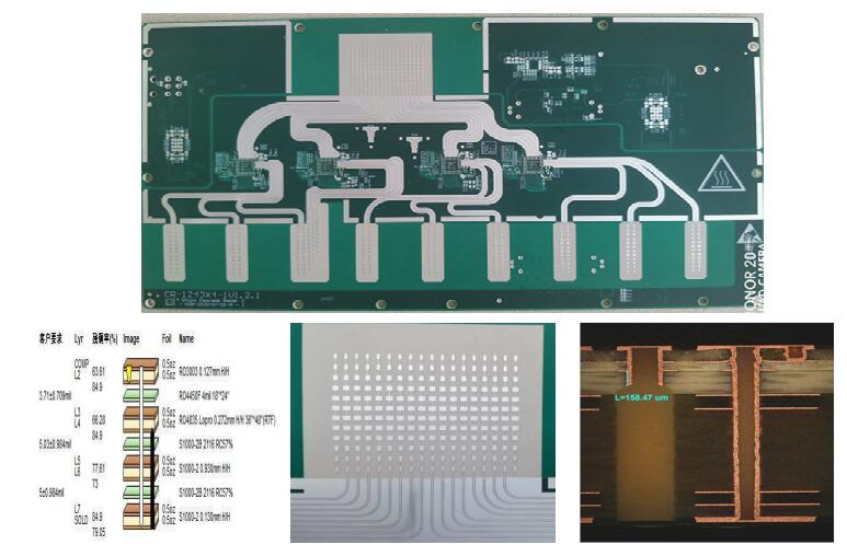
Advanced capabilities in HDI, back drilling, multi-material lamination, impedance control, PoFV, and 77 GHz RF/microwave radar.
| Product Basic Information | Value |
|---|---|
| Number of Layers | 8L |
| Finished Board Thickness | 2.0 ± 0.2 mm |
| Finished Board Size | 11.81 × 6.44 in |
| Aspect Ratio | Through Hole 7:1, Blind Hole 0.63:1 |
| Board Material | MT-77 + RO4835 LowPro + S1000-2 Hybrid Lamination |
| Minimum Drill / Finished Hole | 0.275 / 0.2 mm |
| Minimum Line Width / Line Spacing | 0.102 / 0.114 mm |
| Back Drilling | Stub Control 8 mil |
| Impedance Tolerance | ±10% |
| Surface Finish | Immersion Silver (ImAg) |
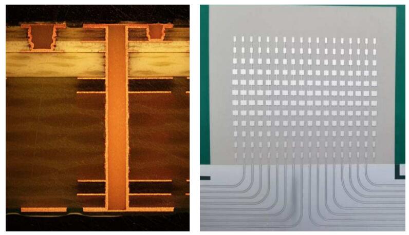
Advanced PCB capabilities including HDI with L1–L3 laser-drilled microvias, back drilling, multi-material hybrid lamination, precise impedance control, PoFV packaging process, and 77 GHz RF/microwave radar applications.
| Product Basic Information | Value |
|---|---|
| Number of Layers | 10L |
| Finished Board Thickness | 1.4 ± 0.14 mm |
| Finished Board Size | 15.66 × 12.24 in |
| Aspect Ratio | Through Hole 5.4:1, Blind Hole 0.93:1 |
| Board Material | RO3003 + R5785 Hybrid Lamination |
| Minimum Drill / Finished Hole | 0.25 / 0.2 mm |
| Minimum Line Width / Line Spacing | 0.13 / 0.1 mm |
| Back Drilling | N/A |
| Impedance Tolerance | ±10% |
| Surface Finish | OSP (Organic Solderability Preservative) |
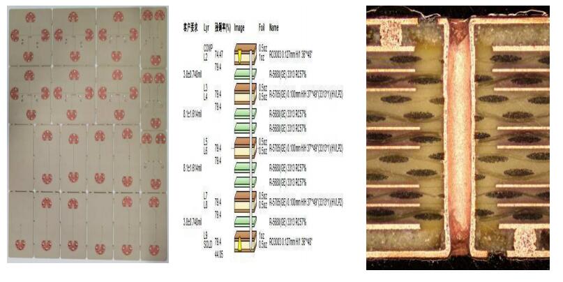
Advanced PCB capabilities including large-panel design, HDI structures, microwave RF boards, high-frequency multi-material hybrid lamination with plated-through hole filling, and steam car boards for 77 GHz RF/microwave radar applications.
| Product Basic Information | Value |
|---|---|
| Number of Layers | 8L |
| Finished Board Thickness | 1.6 ± 0.16 mm |
| Finished Board Size | 5.98 × 3.94 in |
| Aspect Ratio | Through Hole 6:1, Blind Hole 0.58:1 |
| Board Material | RO4835 + IT180A Hybrid Lamination (n+n structure) |
| Minimum Drill / Finished Hole | 0.25 / 0.2 mm |
| Minimum Line Width / Line Spacing | 0.102 / 0.114 mm |
| Back Drilling | N/A |
| Impedance Tolerance | ±10% |
| Surface Finish | Immersion Nickel/Gold (ENIG) |
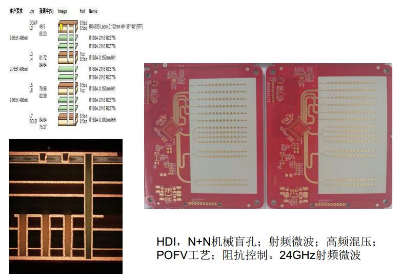
Advanced PCB capabilities including HDI with N+n mechanical blind vias, RF/microwave design, high-frequency multi-material hybrid lamination, PoFV packaging process, impedance-controlled design, and 24 GHz RF/microwave applications.
| Product Basic Information | Value |
|---|---|
| Number of Layers | 6L |
| Finished Board Thickness | 1.6 ± 0.16 mm |
| Finished Board Size | 6.79 × 5.08 in |
| Aspect Ratio | Through Hole 5.9:1, Blind Hole 0.58:1 |
| Board Material | RO4835 + IT180A |
| Minimum Drill / Finished Hole | 0.25 / 0.2 mm |
| Minimum Line Width / Line Spacing | 0.102 / 0.114 mm |
| Back Drilling | N/A |
| Impedance Tolerance | ±10% |
| Surface Finish | Immersion Nickel/Gold (ENIG) |
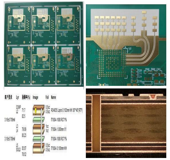
Expertise in HDI, PoFV, impedance control, hybrid lamination, and 24 GHz RF/microwave PCB applications.
| Product Basic Information | Value |
|---|---|
| Number of Layers | 8L |
| Finished Board Thickness | 1.64 ± 0.17 mm |
| Finished Board Size | 13.78 × 12.81 in |
| Aspect Ratio | Through Hole 6.1:1, Mechanical Blind Hole 1.17:1 |
| Board Material | S7135 + IT180A Hybrid Lamination |
| Minimum Drill / Finished Hole | 0.25 / 0.2 mm |
| Minimum Line Width / Line Spacing | 0.5 / 0.127 mm |
| Back Drilling | Three types of mechanical drilling with PTH depth control |
| Impedance Tolerance | N/A |
| Surface Finish | Immersion Silver (ImAg) |
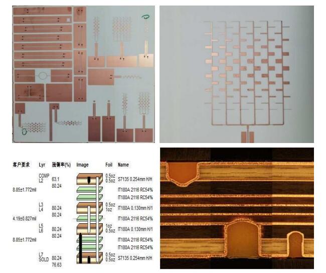
Advanced PCB capabilities including large-panel design, mechanical blind vias, microwave RF boards, multi-material hybrid lamination, and back drilling with varying depths.
| Product Basic Information | Value |
|---|---|
| Number of Layers | 14L |
| Finished Board Thickness | 2.5 ± 0.25 mm |
| Finished Board Size | 21.73 × 10.91 in |
| Aspect Ratio | 9.8:1 |
| Board Material | TU-862HF + S7135 |
| Minimum Drill / Finished Hole | 0.25 / 0.2 mm |
| Minimum Line Width / Line Spacing | 0.114 / 0.114 mm |
| Back Drilling | Double-sided back drilling; stub height in the same hole controlled at 8 mil |
| Impedance Tolerance | ±10% |
| Surface Finish | Immersion Nickel/Gold (ENIG) |
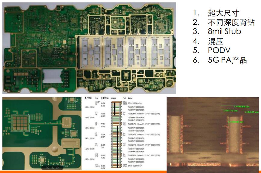
Expertise in oversized PCBs, multi-depth back drilling (8 mil stub), hybrid lamination, PoDV process, and 5G PA PCB solutions.
// Frequently Asked Questions (FAQ)High-Frequency PCBs FAQ
High Frequency PCB and RF Microwave PCB are special types of PCBs designed to handle high-frequency and high-speed signals, commonly used in communication and high-performance electronic devices. Here are their definitions and characteristics:
High Frequency PCB
Definition: High Frequency PCBs generally refer to those operating at frequencies above 1GHz, mainly used for transmitting high-frequency signals.
Characteristics:
- Material Selection: Typically use special materials with low loss and stable dielectric constants, such as PTFE (polytetrafluoroethylene), ceramic substrates, or high-performance FR-4.
- Low Loss: Ensure low signal loss at high frequencies, maintaining signal integrity.
- Stable Dielectric Constant: Maintain stability across different frequencies and temperatures, reducing signal distortion.
- Thermal Management: Effective thermal management to handle the heat generated by high-frequency operation.
- Accurate Impedance Control: Precise design and manufacturing to ensure the characteristic impedance of the traces meets design specifications.
Applications:
- Communication systems (e.g., base stations, wireless devices)
- Radar systems
- Navigation systems
- High-speed data transmission equipment
RF Microwave PCB
Definition: RF Microwave PCBs are used for handling radio frequency (RF) and microwave signals, typically operating in the frequency range of 300MHz to 300GHz.
Characteristics:
- High-Frequency Performance: Handle extremely high-frequency signals with excellent frequency response.
- Low Dielectric Loss: Use low-loss dielectric materials, such as PTFE, ceramic substrates, or special composites, to minimize signal attenuation.
- Precision Manufacturing: Require highly precise manufacturing processes to ensure the integrity and consistency of signal paths.
- Strict Impedance Control: Maintain strict impedance control to minimize signal reflection and loss.
- Thermal Stability: Materials remain stable at high temperatures to handle the thermal stress of high-frequency operations.
Applications:
- Wireless communication devices (e.g., smartphones, Wi-Fi routers)
- Satellite communications
- Radar and navigation systems
- Microwave communication
- Medical devices (e.g., MRI)
Key Differences
While both High Frequency PCBs and RF Microwave PCBs are capable of handling high-frequency signals, RF Microwave PCBs typically deal with much higher frequencies and require more stringent material and manufacturing process requirements to ensure stable and reliable performance at extremely high frequencies.
High frequency PCBs differ from regular PCBs primarily in their design and material considerations to accommodate signals at high frequencies. Here are the key differences:
- Substrate Material: High frequency PCBs use specialized substrate materials with low dielectric constant (εr) and low loss tangent (δ), such as PTFE (Polytetrafluoroethylene) or ceramic-filled hydrocarbons. These materials minimize signal loss and impedance mismatch at high frequencies.
- Thickness Control: High frequency PCBs often require tighter control over the thickness of the substrate and copper layers to maintain consistent impedance across the board. Variations in thickness can cause signal integrity issues at high frequencies.
- Copper Cladding: They may use thicker copper cladding or different types of copper (e.g., rolled annealed copper) to handle higher current densities and reduce skin effect losses at high frequencies.
- Trace Geometry: High frequency PCBs employ controlled impedance traces with specific widths and spacings to match the characteristic impedance required by the design. This ensures signal integrity and minimizes reflections.
- Dielectric Constant and Loss Tangent: The dielectric constant (εr) and loss tangent (δ) of the substrate material are critical at high frequencies. Lower values of εr and δ reduce signal loss and ensure more efficient transmission of signals.
- Surface Finish: The choice of surface finish on high frequency PCBs is crucial to maintain signal integrity and reliability. ENIG (Electroless Nickel Immersion Gold) or immersion silver finishes are commonly used due to their flatness and good electrical properties.
- Design Considerations: High frequency PCB design involves careful consideration of signal paths, via structures, and component placement to minimize parasitic effects, such as parasitic capacitance and inductance, which can affect high-frequency performance.
In summary, high frequency PCBs are optimized to handle signals in the GHz range with minimal loss and distortion, requiring specialized materials, precise manufacturing processes, and meticulous design considerations compared to regular PCBs used for lower frequency applications.
High-frequency PCB materials are primarily used in high-frequency and high-frequency signal environments to provide excellent electrical and thermal performance. Here are some common high-frequency PCB materials and their characteristics:
- PTFE (Polytetrafluoroethylene) Based Materials PTFE is a material with extremely low dielectric constant and loss factor, making it ideal for high-frequency applications.
- Characteristics: Very low dielectric constant (2.0-2.2), low loss factor, excellent high-frequency performance, high-temperature resistance, good chemical stability.
- Applications: High-frequency communication equipment, radar systems, satellite communications, etc.
- Examples: Rogers RO3000 series, Taconic TLY series.
- Ceramic-Filled PTFE Materials This material is filled with ceramic powder in the PTFE base to enhance mechanical strength and thermal stability while maintaining low dielectric constant and low loss.
- Characteristics: Low dielectric constant, low loss, high mechanical strength, and thermal stability.
- Applications: High-frequency and microwave applications requiring higher mechanical strength and thermal performance.
- Examples: Rogers RO4000 series, Arlon AD series.
- High-Performance FR-4 Materials Improved FR-4 materials optimize the ratio of resin and glass fiber cloth to provide a lower dielectric constant and loss factor, offering cost efficiency.
- Characteristics: Lower dielectric constant (generally 3.5-4.0), lower loss factor, high cost efficiency.
- Applications: Medium to high-frequency communication equipment, high-frequency applications sensitive to cost.
- Examples: Isola FR408HR, Nelco N4000-13 series.
- Ceramic-Based Materials Ceramic-based or ceramic-filled materials have very high thermal conductivity and low dielectric constant, maintaining stable performance at very high frequencies.
- Characteristics: High thermal conductivity, low dielectric constant, extremely low loss.
- Applications: High-power amplifiers, RF modules, high-frequency applications requiring high thermal management.
- Examples: Rogers RT/duroid series, CoorsTek ceramic substrates.
- LCP (Liquid Crystal Polymer) Materials LCP materials have extremely low dielectric constant and loss factor, along with good mechanical properties and thermal stability.
- Characteristics: Very low dielectric constant (around 2.9), low loss factor, good mechanical properties, and thermal stability.
- Applications: High-frequency flexible PCBs, 5G antennas, RFID devices.
- Examples: Rogers ULTRALAM series.
- Composite Materials Composite materials are composed of multiple materials, combining their advantages, such as low loss, high strength, and high thermal conductivity.
- Characteristics: Excellent overall performance, low loss, high strength, high thermal conductivity.
- Applications: High-frequency applications requiring comprehensive performance.
- Examples: Rogers TMM series, Arlon TC350 series.
Choosing the right high-frequency PCB material is crucial to ensure the performance and reliability of the circuit board in high-frequency environments. Different materials are suitable for different application scenarios, and selecting according to specific needs can maximize the performance and cost efficiency of the circuit board.
- ENIG (Electroless Nickel Immersion Gold)
- Process: Chemical nickel is deposited on the PCB surface followed by immersion in a gold solution to form a metallic gold layer.
- Features: Provides a flat, smooth surface suitable for high-frequency circuits, with good solderability and corrosion resistance.
- HASL (Hot Air Solder Leveling)
- Process: Molten solder is applied over the entire PCB surface, then leveled using hot air.
- Features: Cost-effective, suitable for general PCB manufacturing, but may introduce some loss for high-frequency PCBs.
- Immersion Tin
- Process: PCBs are immersed in a tin salt solution to form a tin layer.
- Features: Provides a flat surface, suitable for high-frequency and digital signal transmission.
- Immersion Silver
- Process: PCBs are immersed in a silver solution to deposit a silver layer.
- Features: Offers excellent electrical performance and good corrosion resistance, suitable for high-frequency applications.
- OSP (Organic Solderability Preservatives)
- Process: Forms an organic protective layer on the PCB surface through chemical means.
- Features: Simple, low-cost, suitable for soldering requirements of high-frequency PCBs.
- ENEPIG (Electroless Nickel Electroless Palladium Immersion Gold)
- Process: Chemical nickel is first deposited, followed by a palladium layer, and then immersion in a gold solution.
- Features: Provides excellent electrical performance and corrosion resistance, suitable for complex high-frequency and high-reliability applications.
Choosing the appropriate surface treatment process is crucial for the performance and reliability of high-frequency PCBs. The specific selection should be based on PCB design requirements, application environment, and performance needs, followed by comprehensive consideration and testing validation.
Testing high frequency PCBs involves a combination of specialized techniques to ensure signal integrity, impedance control, and overall performance. Here are the key methods used:
- Time Domain Reflectometry (TDR):
- Purpose: Measures impedance along a trace to identify mismatches, discontinuities, and other anomalies.
- Process: A fast-rise time pulse is sent through the PCB trace, and reflections are analyzed to detect impedance variations.
- Vector Network Analysis (VNA):
- Purpose: Measures the network parameters (S-parameters) of the PCB, providing information about reflection (S11, S22) and transmission (S21, S12) characteristics.
- Process: The VNA applies high-frequency signals and measures the response, helping to identify losses, phase shifts, and impedance characteristics.
- Insertion Loss Testing:
- Purpose: Evaluates the loss of signal power as it travels through the PCB traces and interconnections.
- Process: High-frequency signals are injected into the PCB, and the output is measured to determine the amount of signal attenuation.
- Return Loss Testing:
- Purpose: Assesses the amount of signal reflection due to impedance mismatches along the transmission lines.
- Process: Similar to TDR, but focuses on measuring the reflected signals and calculating the return loss.
- Cross-Talk Testing:
- Purpose: Detects electromagnetic interference between adjacent traces on the PCB.
- Process: Signals are sent through one trace, and induced signals are measured on adjacent traces to quantify the level of crosstalk.
- Impedance Testing:
- Purpose: Verifies that the PCB traces have the correct characteristic impedance as designed.
- Process: Using TDR or VNA, the impedance of the traces is measured and compared against the design specifications.
- High-Frequency Signal Testing:
- Purpose: Ensures the PCB can handle high-frequency signals without degradation.
- Process: High-frequency signals are transmitted through the PCB, and the output is analyzed for any distortions, noise, or signal integrity issues.
- Electromagnetic Interference (EMI) Testing:
- Purpose: Ensures that the PCB does not emit or is not susceptible to electromagnetic interference.
- Process: EMI testing is conducted in an anechoic chamber where emissions are measured, and the PCB’s susceptibility to external EMI is tested.
- Thermal Testing:
- Purpose: Evaluates the thermal performance and heat dissipation capabilities of the PCB.
- Process: The PCB is subjected to high-frequency operation, and thermal imaging or temperature sensors are used to measure heat distribution and identify hotspots.
- Functional Testing:
- Purpose: Verifies that the PCB operates correctly within the intended system or device.
- Process: The PCB is integrated into the final product or a test fixture, and its functionality is tested under various operational conditions.
- Environmental Testing:
- Purpose: Ensures reliability under different environmental conditions, such as temperature, humidity, and vibration.
- Process: The PCB is subjected to environmental stress tests to simulate real-world operating conditions and ensure durability and performance stability.
By employing these testing techniques, manufacturers can ensure that high frequency PCBs meet stringent performance and reliability standards required for advanced electronic applications.
High-frequency PCBs are utilized in various industry sectors, including but not limited to:
- Telecommunications:Used in the manufacturing of high-frequency and microwave antennas, transmitters, and receivers, such as 5G base station equipment and satellite communication systems.
- Radar Systems:Employed in the production of radar receivers and signal processing systems, ensuring the stable transmission and processing of high-frequency signals.
- Medical Equipment:Applied in medical imaging devices (e.g., MRI and CT scanners) and other high-frequency electronic medical equipment, ensuring accurate signal transmission and processing.
- Military and Defense:Used in military radar, communication devices, and electronic warfare systems, ensuring the reliability and security of high-frequency signal processing.
- Aerospace:Utilized in communication, navigation, and control systems in aviation and spacecraft, ensuring high-frequency signal transmission and stability in extreme environments.
- Automotive Electronics:Applied in automotive radar, Advanced Driver Assistance Systems (ADAS), and in-vehicle communication systems, supporting high-frequency signal processing and transmission.
- Industrial Automation:Used in high-frequency sensors, wireless communication modules, and industrial control systems, enhancing data transmission rates and system stability.
- Consumer Electronics:Found in high-frequency radio devices, smartphones, and gaming consoles, supporting high-speed data transmission and wireless communication functions.
High-frequency PCBs, due to their excellent electrical performance and signal stability, are widely applied in various technologies and industries that require the handling of complex high-frequency signals and data.
Designing high frequency PCBs presents several challenges due to the nature of signals operating at GHz frequencies. These challenges include:
- Signal Integrity: Maintaining signal integrity is crucial at high frequencies to minimize signal loss, reflections, and electromagnetic interference (EMI). Designers must carefully control impedance, minimize parasitic capacitance and inductance, and optimize signal paths.
- Material Selection: Choosing the right substrate material with low dielectric constant (εr) and low loss tangent (δ) is critical. High frequency PCBs often use materials like PTFE (e.g., Rogers RO4003) or specialty laminates with controlled characteristics to ensure minimal signal attenuation and distortion.
- Trace Geometry and Impedance Control: Designing controlled impedance traces requires precise calculations and layout considerations. Trace widths, spacing, and layer stackups must be optimized to match the required characteristic impedance (Z0) throughout the PCB.
- Crosstalk: At high frequencies, signals can induce crosstalk between adjacent traces due to electromagnetic coupling. Design techniques such as increasing spacing between sensitive signals, using shielding, or employing differential signaling are used to mitigate crosstalk.
- Via Design: Vias introduce parasitic capacitance and inductance, which can affect high frequency signal transmission. High frequency PCBs often require minimized via stubs, proper via placement, and sometimes specialized via structures like microvias to maintain signal integrity.
- Grounding and Power Distribution: Proper grounding and power distribution are crucial to minimize noise and ensure stable voltage supply to active components. High frequency designs often require dedicated ground planes, split planes, and careful placement of decoupling capacitors.
- Manufacturability: High frequency PCBs demand tight tolerances and precision during manufacturing processes such as etching, drilling, and plating. Material handling and substrate preparation are critical to maintain the desired electrical properties.
- Thermal Management: Power dissipation in high frequency circuits can lead to localized heating. Effective thermal management strategies, such as thermal vias, heat sinks, or controlled copper pour areas, are necessary to prevent overheating and ensure reliable operation.
- EMI/EMC Compliance: High frequency PCBs must meet stringent electromagnetic compatibility (EMC) standards to prevent interference with other electronic devices and to operate reliably in electromagnetic environments.
- Testing and Validation: Validating high frequency PCB designs involves specialized testing techniques, such as time domain reflectometry (TDR) and network analysis, to verify impedance matching, signal integrity, and overall performance at high frequencies.
In summary, designing high frequency PCBs requires expertise in electromagnetic theory, material science, signal integrity principles, and careful attention to detail throughout the design and manufacturing process to achieve optimal performance and reliability.
To choose a professional high-frequency PCB manufacturer for producing PCBs, consider the following factors:
- Experience and Expertise:
- Ensure the PCB manufacturer has extensive experience and expertise in high-frequency PCB manufacturing.
- Assess their capabilities in high-frequency circuit design, material selection, and production processes.
- Technical Capabilities:
- Verify if the PCB manufacturer possesses advanced manufacturing equipment and technologies.
- Confirm their ability to meet the requirements for complex high-frequency PCBs, such as precise wiring, small drill sizes, and high-density assembly.
- Quality Control and Certifications:
- Ensure the manufacturer has a robust quality control system in place, compliant with international standards and certifications like ISO 9001.
- Check for industry-specific quality certifications such as IPC standards or customer-specific requirements.
- Material Selection and Supply Chain:
- Evaluate their expertise in high-frequency PCB material selection and management of the supply chain.
- Ensure they can provide suitable high-frequency PCB materials that meet your application requirements, ensuring material consistency and reliability.
- Technical Support and Services:
- Assess the level of technical support and after-sales service offered by the PCB manufacturer.
- Ensure they can provide timely and professional support during design validation, prototype development, and mass production stages.
- Cost-effectiveness:
- Compare quotes and cost structures from different PCB manufacturers.
- Consider not only the lowest price but also the overall quality and service provided for the best cost-effectiveness.
By carefully considering these factors, you can choose a suitable high-frequency PCB manufacturer to ensure the production of high-quality PCB products that meet your requirements.

