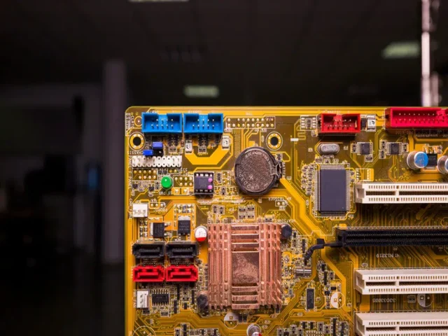
Autonomous UAV flight control systems demand high power density PCB designs capable of handling dense interconnects, high-frequency control signals, and EMI-sensitive power circuits. Compact UAV architectures leave minimal space for routing, making multilayer PCB stackups essential for maintaining signal fidelity, phase stability, and electromagnetic compatibility.
Multilayer UAV PCBs enable segregated power and control planes, optimized EMI shielding, and low-loss RF routing to ensure reliable autonomous navigation, efficient power handling, and robust sensor integration.
Core Engineering Challenges
| Challenge | Root Cause | Engineering Impact |
|---|---|---|
| Power density limitations | Compact UAV PCB footprint | Reduced current handling, thermal hotspots |
| EMI interference | High-frequency motor control signals | Degraded sensor accuracy, GPS drift |
| Crosstalk in high-speed traces | Dense routing, insufficient isolation | Signal distortion, flight control instability |
| Thermal-induced phase drift | CTE mismatch, high power circuits | Misalignment in RF and control signal timing |
| Mechanical stress in UAV frame | Vibration and shocks | Microcracks, layer delamination |
Material Science & Multilayer UAV PCB Advantages
| Parameter | Typical Value / Feature | Engineering Benefit |
|---|---|---|
| Layer count | 6–12 layers | Separates power, signal, and ground planes |
| Dielectric Dk/Df | Low-loss, thermally stable | Maintains phase-stable RF and control signal routing |
| Copper thickness | 0.5–2 oz | Supports high current density and power efficiency |
| Shielding & ground planes | Embedded segmented grounds | Reduces EMI and crosstalk across dense traces |
| Thermal vias & planes | Optimized for heat dissipation | Prevents hotspots, ensures UAV reliability |
KKPCB Case Study — UAV Flight Control PCB

Client Context:
A commercial UAV manufacturer required a multilayer PCB capable of supporting high-power motor control, RF telemetry, and sensor fusion circuits with strict EMI and phase-stability requirements.
KKPCB Solution:
-
8-layer UAV PCB stackup with segregated power, RF, and ground planes
-
Embedded thermal vias and copper planes to enhance heat dissipation
-
Shielded high-speed traces to suppress EMI between control and telemetry signals
-
Controlled impedance and phase-stable routing for RF telemetry and GPS
-
HFSS & TDR simulations to ensure signal integrity and timing precision
Measured Results:
| Parameter | Target | KKPCB Result |
|---|---|---|
| Power Handling | High-density | Fully met |
| Phase Deviation | <0.5° | 0.43° |
| EMI Suppression | >30% | 36% |
| Insertion Loss | Minimal | 0.28 dB/in |
| Thermal Rise | <8°C per layer | 6.7°C |
Stackup Design & Simulation
-
HFSS Modeling: Optimized high-speed and RF trace layout
-
ADS & TDR: Verified phase stability across UAV telemetry lines
-
Thermal FEM: Ensured uniform heat distribution, preventing hotspots
-
AOI & Solder Reflow Monitoring: ±10 µm layer alignment maintained
Environmental & Reliability Validation
| Test | Condition | Result |
|---|---|---|
| Thermal Cycling | –40°C ↔ +85°C, 500 cycles | Phase-stable, no delamination |
| Vibration & Shock | 5–500 Hz, 10G | No microcracks, signal integrity intact |
| Humidity & Moisture Testing | 85°C / 85% RH, 500 h | Dielectric stable, no EMI increase |
| High-Power Operation | Continuous flight cycles | Minimal insertion loss (<0.03 dB) |
| Solder Reflow | 260°C ×3 cycles | Stackup alignment maintained |
Engineering Summary & Contact
Multilayer UAV PCB stackups provide high power density, EMI-controlled, phase-stable, and low-loss routing for autonomous flight control systems. KKPCB’s precision stackup design, thermal management, and EMI mitigation strategies deliver reliable UAV operation, accurate sensor fusion, and stable telemetry even in harsh environmental conditions.
Contact KKPCB Engineering Team for multilayer UAV PCB design consultation, RF signal simulation, and thermal/EMI performance validation for your next-generation drone platform.
