Meeting the Demands of High-Speed Data Transmission
With the rapid growth of data communication systems, the need for high-performance and reliable data transmission modules is increasing. These modules require advanced PCB design, precise PCB assembly (PCBA), and strict quality control to ensure stable high-speed signal transmission.
A customized PCBA manufacturing solution is essential to meet the unique requirements of each data transmission module, especially in applications such as telecommunications, industrial networking, and high-speed computing systems.
Project Background: Customer Requirements
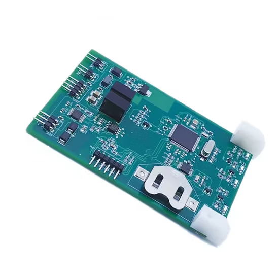
The client required a customized PCBA solution for a high-speed data transmission module with the following specifications:
- High-speed signal integrity requirements
- Compact PCB layout design
- Stable performance under continuous operation
- Strict quality and reliability standards
The project demanded a tailored PCB manufacturing and assembly solution to ensure optimal performance.
Key Challenges in PCBA Manufacturing
1. High-Speed Signal Integrity
Maintaining signal integrity in a data transmission module is critical.
- Risk of signal loss and crosstalk
- Need for controlled impedance routing
- High-frequency performance requirements
2. High-Density PCB Layout
The module required a compact multilayer PCB design:
- Limited space for component placement
- Complex routing requirements
- High-density SMD assembly
3. Thermal Management
Continuous operation generates heat, requiring:
- Efficient thermal dissipation design
- Stable performance under load
4. Manufacturing Precision
High-speed designs require strict PCB fabrication and assembly control:
- Tight tolerances
- Accurate component placement
- Consistent soldering quality
Customized PCBA Manufacturing Solution
1. Advanced PCB Design Optimization
We optimized the PCB layout to enhance signal integrity:
- Controlled impedance routing
- Shortened signal paths
- Reduced crosstalk and EMI
2. Multilayer PCB Stack-Up Design
A carefully engineered multilayer PCB stack-up ensured:
- Stable electrical performance
- Balanced signal layers
- Improved power integrity
3. High-Precision PCB Fabrication
Our PCB manufacturing process included:
- Tight control of trace width and spacing
- High-quality materials for high-speed PCB applications
- Precision drilling and plating
4. Advanced SMT Assembly Process
For PCB assembly (PCBA), we implemented:
- High-accuracy SMT placement
- Optimized reflow soldering profile
- Strict solder paste control
5. Comprehensive Testing and Validation
To ensure reliability, we performed:
- AOI and X-ray inspection
- Electrical testing (E-test)
- Functional testing of the data transmission module
Results and Performance Improvements
After implementing the customized PCBA solution, the customer achieved:
- Improved signal integrity and reduced signal loss
- Stable high-speed data transmission performance
- Enhanced thermal stability
- Increased production yield and consistency
The optimized PCBA manufacturing process ensured long-term reliability of the module.
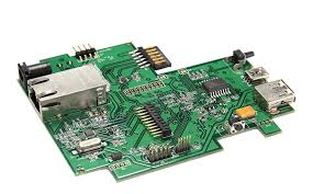
Applications of the Data Transmission Module
The customized PCBA solution is suitable for:
- Telecommunication equipment
- Industrial networking systems
- Data centers and servers
- High-speed communication devices
These applications require high-performance PCB assembly solutions.
Why Choose a Customized PCBA Manufacturing Solution?
A customized PCBA approach offers:
- Tailored PCB design and assembly
- Improved performance and reliability
- Faster time-to-market
- Better cost control in mass production
Conclusion: Delivering High-Performance PCBA Solutions
A well-executed customized PCBA manufacturing solution is essential for high-speed data transmission modules. By combining advanced PCB design, precision manufacturing, and rigorous testing, manufacturers can deliver reliable and high-performance PCBA products.
Customized solutions ensure that each project meets its specific requirements, enabling success in competitive high-speed communication markets.
