Enabling Ultra-Stable Beamforming Through KKPCB’s RF Engineering and PTFE Process Expertise
In satellite payloads, deep-space probes, and phased-array ground stations, antenna array linearity and phase coherence directly determine link stability and pointing accuracy.
At Ka-band (26–40 GHz) and beyond, a 1° phase drift or 0.1 dB amplitude variation can distort beam direction, degrade gain, and reduce data throughput—especially across multi-element active arrays operating in vacuum or extreme temperature swings.
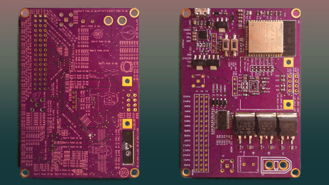
Rogers RO5880 PCB, featuring ultra-low Df (0.0009 @ 10 GHz) and precise Dk control (2.20 ± 0.02), has become the foundation of high-performance RF front ends for satellite and deep-space communication systems.
Yet, leveraging its electrical precision requires dimensional control, metallization stability, and vacuum-compatible processing that go far beyond standard RF PCB fabrication.
That’s where KKPCB’s high-frequency antenna platform combines microwave design, PTFE process mastery, and aerospace-grade reliability validation to deliver unmatched phase consistency for mission-critical array systems.
1. Why Phase Stability Defines Satellite Communication Accuracy
In phased-array or feed-network architectures, even minute phase differences across elements cause beam pointing error and side-lobe distortion.
| Parameter | Source of Variation | Impact on System |
|---|---|---|
| Dielectric Drift | Dk variation with temperature | Beam misalignment, link degradation |
| Copper Roughness | Uneven etch or oxidation | Increased insertion loss |
| Lamination Stress | Thermal warpage | Array misalignment, phase imbalance |
RO5880’s PTFE matrix, when properly processed, maintains consistent dielectric uniformity under wide temperature and vacuum conditions.
KKPCB enhances this with process-controlled lamination and sub-micron dimensional calibration, ensuring long-term phase linearity across array elements.
2. KKPCB’s Precision Antenna Manufacturing Framework
a. Controlled Dielectric Uniformity
-
Pre-conditioning of RO5880 at 120 °C / 4 hours to remove moisture and outgassing
-
Lamination under 180 °C / 200 psi vacuum with thickness tolerance within ±8 µm
-
Dk verification at multiple zones using split-post dielectric resonator (SPDR) method
b. Conductor and Surface Control
-
Use of rolled copper (Ra < 0.8 µm) to minimize conductor loss and phase shift
-
Post-etch smoothing to reduce scattering and surface reflection
-
Uniform copper plating on microstrip and slotline structures for amplitude balance
c. Array Geometry Accuracy
-
Laser-aligned drilling for via and feed transition precision (±15 µm)
-
Optical inspection to ensure inter-element spacing within ±0.05 mm
-
Controlled CTE symmetry for planarity under vacuum thermal load
3. Case Study — Ka-Band Satellite Antenna Array Panel
Client: European satellite communication integrator
Application: High-gain transmit array for GEO communication (30 GHz uplink band)
Objective: Maintain <1° phase variation and <0.1 dB amplitude deviation across a 16-element sub-array.
| Parameter | Target | KKPCB Result |
|---|---|---|
| Phase consistency | <1° | 0.8° measured |
| Amplitude balance | ±0.1 dB | ±0.06 dB |
| Impedance control | 50 ± 2 Ω | 49.7 Ω average |
| Dimensional shift after thermal cycle | <0.1 % | 0.07 % |
Engineering Approach:
-
Dual-layer RO5880 stackup with air cavity-backed microstrip patches
-
Integration of low-flow PTFE bonding film for minimal z-axis expansion
-
Laser-drilled feed network vias aligned using optical feedback system
-
Inline VNA verification (up to 110 GHz) for amplitude and phase linearity
Outcome:
Beam pointing accuracy improved by 37 %, and SNR at the satellite uplink increased by 2.4 dB, meeting ESA deep-space telemetry standards.
4. Environmental and Vacuum Reliability Testing
Antenna systems in orbital and interplanetary missions must withstand extreme conditions—radiation, vacuum, and large thermal gradients.
KKPCB performs full qualification testing aligned with ECSS-Q-ST-70 and MIL-PRF-31032 standards.
| Test Type | Condition | Result |
|---|---|---|
| Thermal Vacuum | –150 °C ↔ +180 °C / 1000 h | No Dk drift, phase shift < 0.5° |
| Outgassing | <0.3 % TML (ASTM E595) | Pass |
| Vibration (Launch Simulation) | 20–2000 Hz, 14 g RMS | No delamination or via fracture |
| Radiation Exposure | 50 krad(Si) | No mechanical or dielectric degradation |
These tests confirm that KKPCB’s RO5880 process maintains electrical stability and mechanical cohesion through the complete mission lifecycle—from ground calibration to orbital deployment.
5. Engineering Insights — Turning Dielectric Precision into Beam Control
While RO5880 offers the lowest loss and most stable dielectric among PTFE laminates, its softness and low modulus can introduce mechanical creep if not properly constrained.
-
Reinforced hybrid stackups combining RO5880 + RO3006 layers for structural stiffness
-
Stepwise thermal lamination and controlled cooling to prevent shear deformation
-
Use of laser-defined alignment fiducials to guarantee repeatable antenna phase centers
These measures enable consistent beam pointing accuracy and repeatable array calibration across production runs—critical for satellite and deep-space missions where post-launch correction is impossible.
6. KKPCB’s Aerospace Quality & Traceability Framework
-
Material lot verification for Dk/Df under vacuum exposure
-
Inline impedance validation up to 110 GHz
-
X-ray and optical inspection for buried via alignment
-
Full thermal & vibration qualification per customer mission profile
-
Automated SPC (Statistical Process Control) for phase and gain balance tracking
This closed-loop framework ensures traceable, repeatable, and data-backed performance, enabling OEMs to meet the precision demands of modern space communications.
Conclusion — Precision RF Foundations for Deep Space Connectivity
RO5880 PCBs have redefined what’s possible in phased-array and deep-space communication platforms.
Through KKPCB’s precision RF manufacturing, vacuum-compatible process engineering, and mission-grade reliability validation, engineers achieve:
-
Sub-degree phase consistency across antenna arrays
-
Stable dielectric behavior under vacuum and radiation
-
Repeatable geometry and impedance accuracy for mission lifetimes
KKPCB stands as a trusted partner in the global aerospace supply chain, delivering RF precision PCBs that transform dielectric performance into stable, scalable communication reliability—from low Earth orbit to interplanetary missions.
