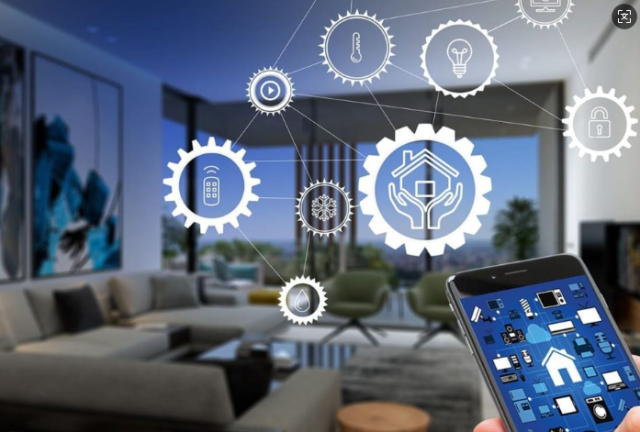
In the era of intelligent living, smart homes are no longer futuristic concepts—they are practical ecosystems built upon seamless electronic integration. At the foundation of every smart device lies a Printed Circuit Board Assembly (PCBA), the vital component that connects sensors, processors, and communication systems into one coherent network.
Smart Home PCB Assembly refers to the engineering and manufacturing process that transforms a bare circuit design into a fully functional module capable of managing automation, sensing, and data communication across an entire household. It is the invisible architecture that enables homes to think, respond, and adapt.
1. The Engineering Foundation of Smart Home PCB Assembly
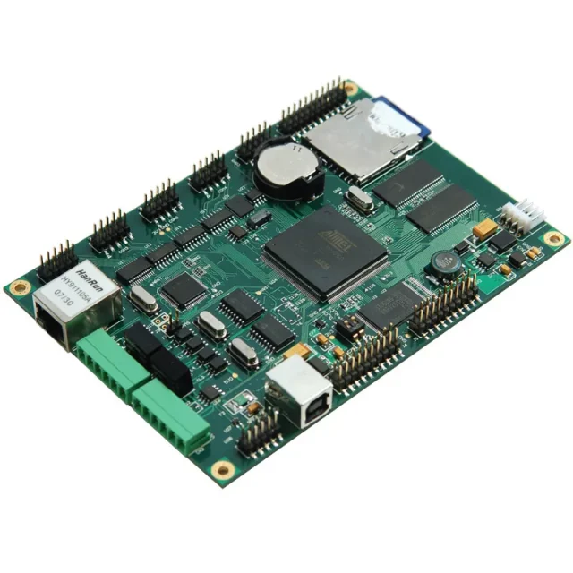
Smart home PCB assemblies are not just electronic boards—they are multi-layered systems integrating signal processing, communication control, and power optimization.
Each PCB must balance electrical performance, thermal management, and EMC (Electromagnetic Compatibility) to ensure stable and interference-free operation.
Engineers select high-Tg FR4, Rogers, or metal-based substrates depending on thermal requirements and circuit density. Surface Mount Technology (SMT) and Through-Hole Assembly (THA) techniques are applied to mount components such as microcontrollers, communication modules, and power ICs with precision. This ensures compact layouts, reduced noise, and high reliability under 24/7 operation.
2. Core Functional Modules in Smart Home PCB Assembly
A modern smart home PCB typically integrates several critical modules that define its performance:
• Automation Control Unit (ACU):
The ACU serves as the “brain” of the system, hosting microcontrollers or embedded SoCs that execute logic control, data processing, and inter-device communication.
• Wireless Connectivity Module:
Wi-Fi, Bluetooth Low Energy (BLE), Zigbee, or Z-Wave modules allow interoperability among devices and cloud platforms, ensuring seamless control via apps or voice assistants.
• Sensor Network:
Temperature, humidity, motion, and light sensors are embedded for real-time environmental monitoring. These sensors feed data into AI-driven algorithms that automate actions—such as adjusting HVAC or lighting conditions.
• Power Management System:
To maintain stability and energy efficiency, PCBs incorporate voltage regulators, current limiters, and smart power switches. In battery-powered devices, charging ICs and low-dropout regulators (LDOs) extend battery life and ensure safe operation.
• Security Subsystem:
Encryption ICs, authentication chips, and secure boot circuits protect communication channels and prevent data tampering—ensuring user privacy and system integrity.
3. Types of Smart Home PCB Assemblies
Depending on application scenarios, PCB assemblies can take many specialized forms:
-
Lighting Control PCBA: Enables intelligent dimming, color temperature control, and motion-activated lighting.
-
Thermostat Control PCBA: Regulates HVAC performance through adaptive temperature sensing.
-
Security & Surveillance PCBA: Powers alarm systems, motion detection, and real-time monitoring.
-
Automation Hub PCBA: Centralized control boards that connect all smart devices.
-
Voice Assistant PCBA: Integrates microphones, DSPs, and AI processors for voice recognition.
-
Appliance Control PCBA: Enables IoT-driven control for home appliances like washing machines or ovens.
-
Environmental Monitoring PCBA: Tracks CO₂, air quality, and humidity for wellness optimization.
-
Motor Control PCBA: Operates automatic shades, doors, and window systems with precision sensors.
Each design demands specific PCB stack-ups, controlled impedance routing, and EMI shielding to ensure performance consistency across environments.
4. Reliability and Quality Assurance
Smart home devices operate continuously, often in variable conditions. Therefore, reliability is non-negotiable.
During assembly, strict process control is applied to reflow soldering, X-ray inspection, and AOI (Automated Optical Inspection). Functional testing ensures every PCBA meets design specifications before integration into final products.
KKPCB emphasizes IPC-A-610 Class 2/3 compliance, RoHS and REACH environmental standards, and advanced DFM (Design for Manufacturability) review during the prototyping stage to minimize risk and enhance performance consistency.
5. The KKPCB Advantage
At KKPCB, we combine engineering precision, manufacturing expertise, and reliable supply chain management to deliver Smart Home PCB Assemblies that meet global standards.
Our services cover schematic design, PCB layout, component sourcing, SMT assembly, functional testing, and mass production, ensuring one-stop delivery from concept to reality.
With our expertise, clients can accelerate time-to-market, enhance product quality, and innovate confidently within the fast-evolving smart home industry.
