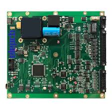
In the world of power electronics, High-Voltage PCB design—typically involving circuits operating above 100V—presents unique challenges that go far beyond standard digital layouts. Designing for high voltage requires a deep understanding of dielectric breakdown, atmospheric conditions, and material science. Failing to implement proper high-voltage safety standards can lead to catastrophic arcing, board carbonization, or complete system failure. Whether you are developing an EV Battery Management System (BMS), a power inverter, or industrial medical equipment, these 8 expert tips will ensure your PCB assembly is both safe and reliable.
1. Master Clearance and Creepage Distances
The foundation of any high-voltage circuit is the physical separation of conductive elements.
- Clearance: The shortest distance through air between two conductive traces. Air acts as an insulator, but its dielectric strength can be compromised by humidity and pressure.
- Creepage: The shortest distance along the surface of the PCB insulation between two traces.
Designers must strictly adhere to IPC-2221B standards to calculate these distances based on peak working voltage and the environment.
2. Select Laminates with High CTI (Comparative Tracking Index)
Standard FR-4 may not suffice for extreme high-voltage applications. The Comparative Tracking Index (CTI) measures the electrical breakdown (tracking) of the insulating material.
- For High-Voltage PCBs, choose materials with a high CTI rating (e.g., CTI > 600) to prevent the formation of conductive carbon paths on the board surface, which is a leading cause of short circuits in power electronics.
3. Implement Isolation Slots and V-Grooves
When board space is limited and you cannot meet the required creepage distance, physical intervention is necessary. By routing isolation slots (air gaps) through the PCB between high-side and low-side sections, you effectively replace a surface path with an air path. Since air generally has a higher dielectric strength than contaminated PCB surfaces, this “air gap” significantly boosts your safety margin.
4. Eliminate Sharp Corners and Utilize Round Geometries
High-voltage electric fields concentrate at sharp points, a phenomenon known as the Corona Effect.
- Avoid 90-degree or 45-degree angles on high-voltage copper traces.
- Use generous curves, teardrops, and rounded pads.
Smooth, circular geometries distribute the electric field more uniformly, preventing localized ionization of the air and reducing the risk of arc-over.
5. Optimize Solder Mask and Conformal Coating
The solder mask acts as the primary defense against oxidation and environmental debris. However, pinholes or “voids” in the mask can become entry points for moisture. For harsh environments, applying a conformal coating is a best practice in high-voltage PCB manufacturing. This adds an extra layer of high-dielectric insulation, protecting the board from dust and humidity that could otherwise trigger an arc.
6. Leverage Multilayer Insulation Strategies
Internal layers of a multilayer PCB offer superior insulation because the prepreg (dielectric) has a much higher breakdown voltage than air.
- Route high-voltage traces on internal layers whenever possible.
- Ensure the “Z-axis” distance (the vertical dielectric thickness between layers) is sufficient to handle the maximum potential difference between overlapping planes.
7. Account for Altitude and Pollution Degrees
As altitude increases, air becomes thinner and its dielectric strength decreases. If your high-voltage PCB is intended for aerospace or high-altitude industrial use, you must “derate” your clearance distances. Additionally, consider the Pollution Degree (1 to 4) of your operating environment; high-pollution areas (dusty or conductive environments) require significantly larger creepage gaps.
8. Rigorous Component Derating and Selection
Never operate components at their absolute maximum voltage ratings. To ensure long-term reliability in power PCB designs, follow a derating rule of at least 20-50%. For a 400V rail, select capacitors, MOSFETs, and connectors rated for 600V or 800V. This overhead allows the system to survive transient voltage spikes and surges without catastrophic failure.
