1. Background Overview
A European client specializing in smart grid and power electronics required a high-precision, compact, and EMI-resistant voltage sensor module PCBA. The solution needed to support multi-channel voltage and current measurement, ensure signal isolation, and be compatible with various control systems.
2. Application Scenario
The PCBA is integrated into power monitoring systems, including inverters, motor drives, and energy management systems. It enables real-time monitoring of voltage and current parameters, ensuring system stability and efficiency in industrial automation applications.
3. Product Specifications
| Parameter | Specification |
|---|---|
| Voltage Measurement Range | ±100V / ±1000V (selectable) |
| Current Measurement Range | ±100A |
| Voltage Bandwidth | DC–100kHz |
| Current Bandwidth | DC–200kHz |
| Output Interfaces | ±10V BNC, 3V/5V IDC |
| Power Supply | 15V DC, 1A |
| Accuracy | 1% |
| Operating Temperature | -25°C to +50°C |
| Dimensions | Compact form factor |
4. Results of Implementation
- Quality: Achieved a 99.8% PCBA pass rate with enhanced soldering reliability.
- Cost: Reduced BOM cost by 12% through component and layout optimization.
- Performance: Improved signal integrity with ±0.1% drift and enhanced EMI shielding.
- Delivery: Shortened lead time from 20 to 12 working days via streamlined processes.
5. KKPCB Advantages Highlighted in This Case
KKPCB offers extensive experience in manufacturing high-precision PCBAs for power electronics and industrial control applications. Our capabilities include:
- Expertise in multi-layer PCB fabrication with strict adherence to IPC standards.
- Advanced SMT and DIP assembly lines ensuring high reliability.
- Comprehensive testing services, including ICT and functional testing.
- Flexible production volumes catering to both prototypes and mass production.
6. KKPCB’s Custom Manufacturing Solution
For this project, KKPCB provided a tailored manufacturing solution focusing on:
- PCB Design Optimization: Implemented a multi-layer design with dedicated ground and power planes to minimize noise and crosstalk.
- Component Placement: Strategically placed high-frequency components to enhance signal integrity.
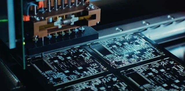
- Assembly Process: Utilized automated SMT lines with precise solder paste application and reflow profiles.
- Quality Assurance: Conducted 100% AOI and X-ray inspections to ensure defect-free assemblies.
- Traceability: Implemented barcode tracking for each PCBA to maintain full production traceability.
7. Real-World Performance Outcomes
Post-implementation, the client reported:
- Enhanced Measurement Accuracy: Voltage and current measurements with 1% accuracy, meeting stringent application requirements.
- Improved System Reliability: Stable operation under varying environmental conditions due to robust design and assembly.
- Cost Efficiency: Overall system cost reduced by 12%, contributing to increased competitiveness.
- Faster Time-to-Market: Accelerated production cycle enabled quicker deployment of end products.
