// PROFESSIONAL ELECTRONIC DESIGN SERVICESPCB Design and Development
From product concept and design to full-scale production, KKPCB is dedicated to providing customers worldwide with comprehensive product development solutions. We earn our clients’ trust through competitive pricing, high quality, and exceptional service. Our complete PCB design capabilities ensure a thorough understanding of your project’s technical requirements and Design for Manufacturability (DFM) principles. Every PCB design we deliver complies with IPC-2220 standards, and our PCB assemblies strictly follow IPC-A-610 quality standards—ensuring precision, reliability, and manufacturability in every product we create.
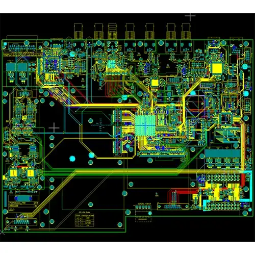
High Frequency PCB Board
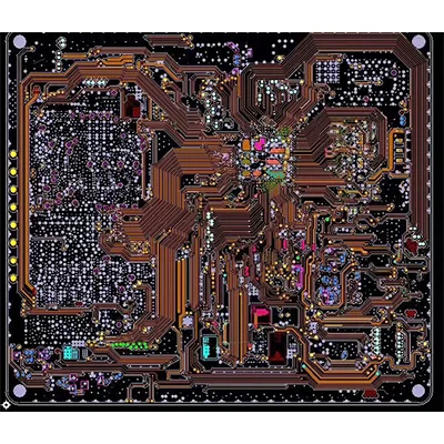
HDI PCB Design
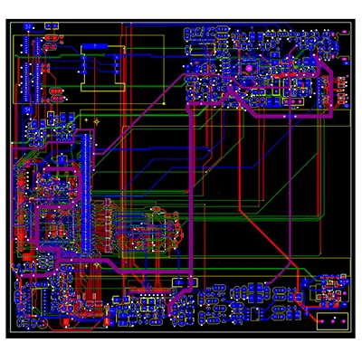
Multilayer PCB Design
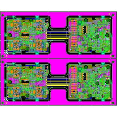
Rigid Flex PCB Design
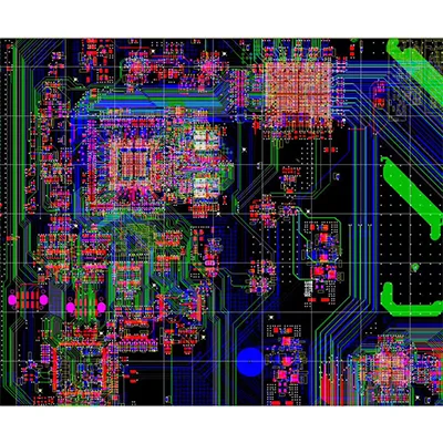
High speed PCB Design
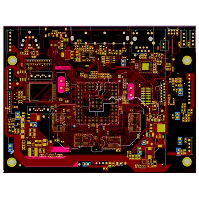
High Power PCB Design
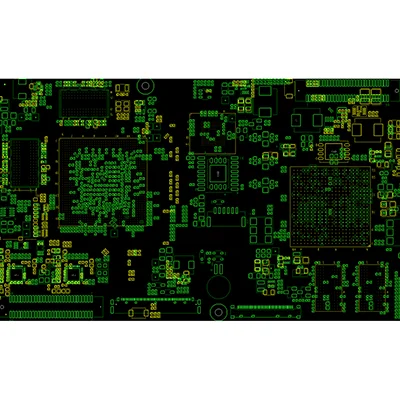
Prototype PCB Design
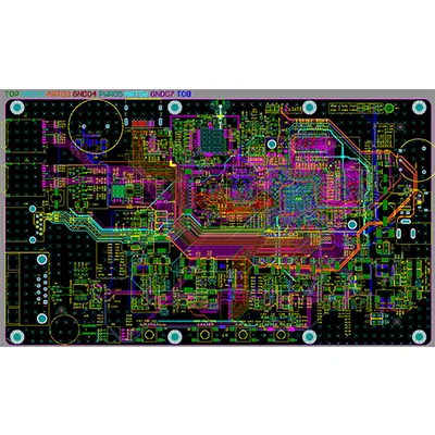
RF PCB Design
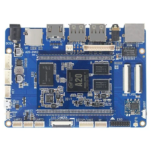
PCB Reverse Engineering
//PCB Design ServicesCUSTOMIZED SERVICE
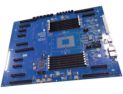
PCB DESIGN AND LAYOUT
At KKPCB, we offer comprehensive PCB design and layout services covering multi-layer rigid, flexible, rigid-flex, and backplane PCBs. Our experienced design engineers specialize in creating complex and high-density layouts with exceptional precision, manufacturability, and signal integrity.
We provide advanced component packaging and library development, including BGA, QFN, and other fine-pitch devices, ensuring seamless integration into your PCB design. Our team has extensive expertise in high-speed PCB design, such as differential pair routing, impedance control, and length matching, as well as high-frequency RF/microwave PCB design for communication and radar systems.
KKPCB also delivers low-level analog and ultra-low EMI designs for sensitive applications such as MRI and medical devices. We are highly experienced in DDR2, DDR3, and DDR4 memory interface design, printed antenna development, high-power circuit design, and thermal/power simulation. In addition, our engineers conduct thorough power integrity (PI) and signal integrity (SI) analyses to ensure reliability and performance under demanding conditions.
Our expertise extends to mixed-signal circuit routing, where precision and noise control are critical. We also provide PCB reverse engineering and redesign services to optimize existing layouts, resolve design issues, or upgrade outdated components using the latest SMT technologies. Through these comprehensive capabilities, KKPCB ensures that every design is optimized for performance, manufacturability, and long-term reliability.
PCB OUTPUT AND PROTOTYPE VERIFICATION
At KKPCB, we provide complete PCB output documentation and prototype verification services to ensure every design is ready for reliable, high-performance manufacturing and assembly. Our engineering team supports customers through every verification stage, from design validation to functional testing and final integration.
Our deliverables and services include:
-
Manufacturing drawings for fabrication and assembly
-
Assembly drawings with component placement and orientation details
-
Gerber and drilling data for precise production
-
Bill of Materials (BOM) and Design Database for accurate sourcing and traceability
-
Customized output files tailored to customer or project-specific requirements
-
PCB and PCBA prototypes for functional evaluation and validation
-
Motherboard testing and verification to ensure full system compatibility
-
Electrical and functional testing, including power, signal integrity, and noise performance tests
-
PCB debugging and modification support for rapid issue resolution
-
Free impedance calculation, stack-up design, QA review, process and EMC inspection to ensure manufacturability and compliance
-
Final product integration and hardware documentation (user manuals, assembly guides, etc.)
-
Post-production support to ensure stable performance and long-term reliability
Through precise documentation, thorough testing, and comprehensive verification, KKPCB ensures that every PCB design transitions seamlessly from prototype to mass production—reducing risk, optimizing quality, and accelerating time-to-market.
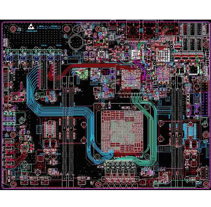
// PCB Design ServicesPCB Design Capabilities
Our PCB design capabilities include:
-
Maximum design layers: up to 64 layers
-
Maximum number of pins: 110,000+
-
Maximum net connections: 78,000+
-
Minimum trace width: 2 mil (0.05 mm)
-
Minimum trace spacing: 2 mil (0.05 mm)
-
Minimum through-hole size: 6 mil (0.15 mm) / 4 mil (0.10 mm) laser via
-
Maximum BGA components per design: 120+
-
Minimum BGA pin pitch: 0.3 mm
-
Maximum BGA pin count: 8,371 pins
-
Maximum signal speed supported: 112G-PAM4
These capabilities enable KKPCB to design and deliver PCBs for advanced electronic systems requiring extreme density, precision, and performance—such as data communication, high-speed computing, aerospace, and next-generation industrial applications.
2. Database data query system, 95% BOM automatic matching
3. All verified through mass production
4. EDA tools
5. Database construction checklist
6. IPC7351 specification
2. Interconversion of PCB libraries for different EDA software
3. Customized project library building service
4. Creating custom schematic symbols
5. Customize and maintain customer-exclusive libraries
2. Memory design (DDR1/2/3/4)
SERDES design (PCIE, SATA, XAUI...)
3. RapidIO 10G BASE-KR, SFI, XFI, CEI-6G, CEI-28G...)
4. High speed backplane design (CPCI, ATCA, VPX...)
2. Communication equipment
3. Consumer
4. Security
5. Monitoring
6. IoT Products
7. Automotive electronics
What is a PCB Layout Design?
A printed circuit board layout design is a very important element that you should consider in designing electronic products.
In many cases, a design engineer is responsible for designing the electronic circuit.
A printed circuit board layout designer is responsible for taking the PCB layout and design from the given schematic.

The PCB layout and design is a special skill that requires you to have knowledge of the basic software.
The type of software that you should have knowledge of is inclusive of the CAD system plus a variety of techniques.
The standards that you will use will ensure a successful transfer of the circuit board to the printed circuit board.
It will also ensure success in the process of manufacturing the printed circuit board in a manufacturing environment.
For a successful manufacture of a printed circuit board, you should have guidelines that you will follow in the process.
There are experts who have experience in the system and are able to design a layout without a guideline.
When it comes to the process of making a printed circuit board design, different software is available for use.
It is important to choose software that many people in the designing industry prefer to use.
Remember, this is an important factor to consider when doing team designs as the software will enhance the skill of engineers.
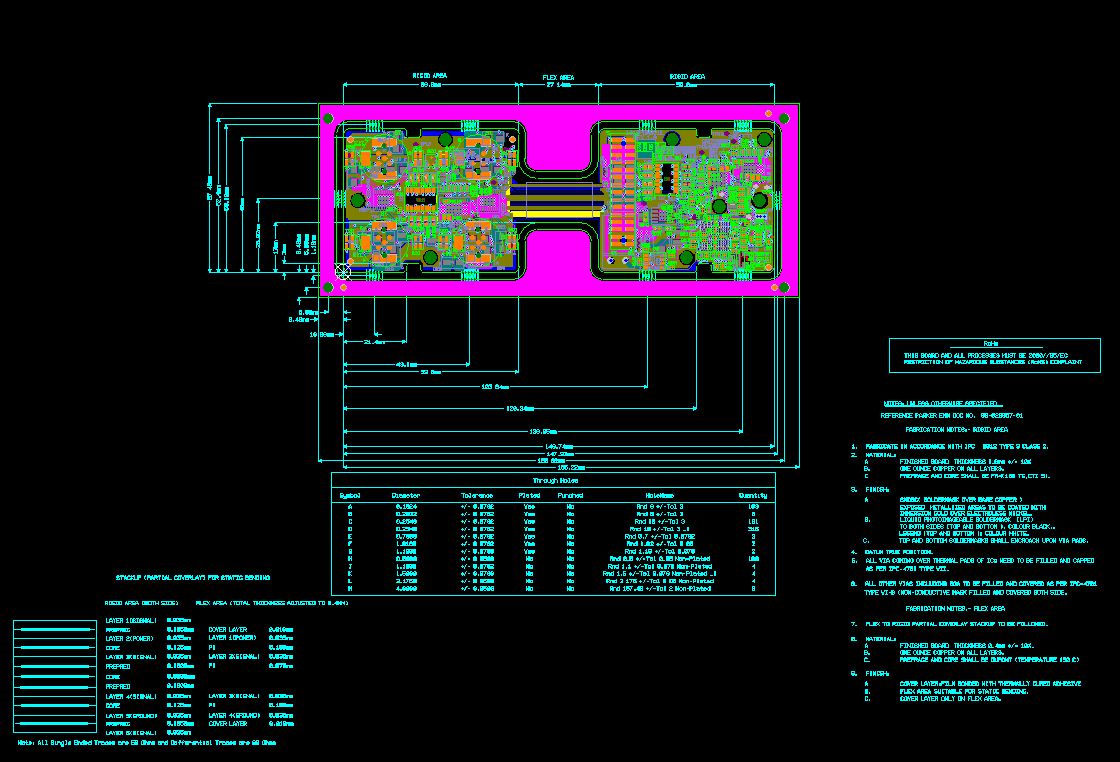
The printed circuit board layout and design software that many people use include Xpedition, PADS, Altium and Cadence Allegro.
The software is suitable for the job of designing the PCB layouts but some do better jobs than others.
The programs that you will use range from simple products to products that have very high sophistication.
Types of PCB Designs
There are quite a number of printed circuit board designs that you can choose from depending on the application.
Continue reading and find out more about the most common types of PCB designs that you can use.
1. Flex PCB Design
A flex PCB design is a type of printed circuit board that is able to bend at different angles.
The material that you will use in making the flex PCB should have the ability to bend round different corners.
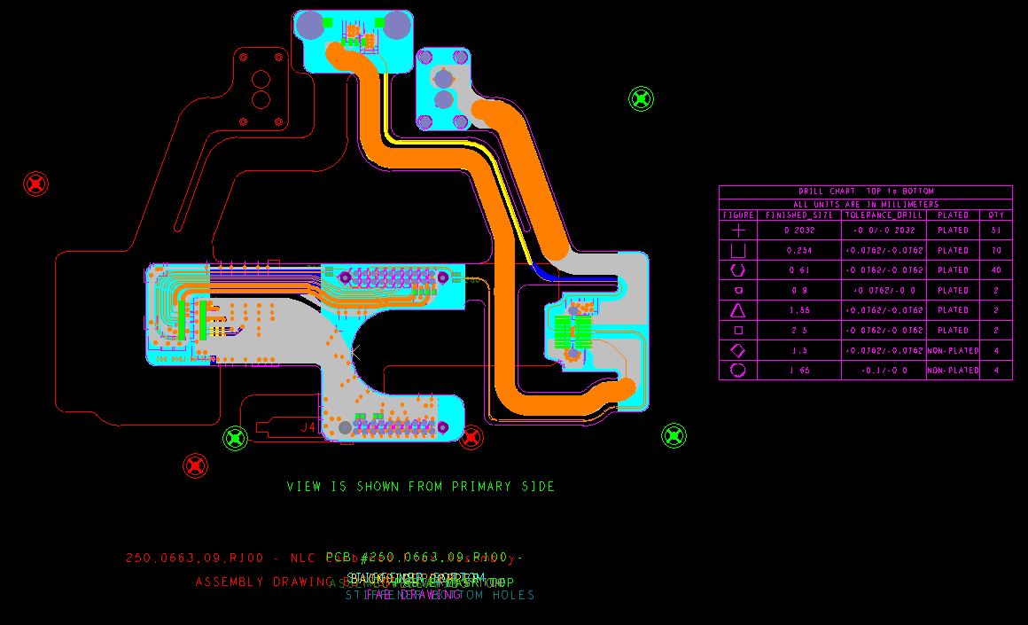
The main materials in a flex PCB design are copper and flexible substrate materials put together using pressure, heat and adhesives.
The substrate that many manufacturers use is the polyimide which is a flexible and strong thermosetting polymer.
Examples of polyimides that you can use are Kapton, Apical, VTEC PI, UPILEX, Kaptrex and Norton TH.
It is, therefore, a pattern of different conductors on an insulating film that is flexible
2. Rigid Flex PCB Design
As the name suggests, it is a printed circuit board with a rigid circuit and a flexible circuit operating together.
The rigid-flex design is important as it has the benefits of the rigid and flexible circuits.
The rigid circuit carries most of the components of the PCB while the flexible area acts as the connections.

The flexible area is meant to save weight and space and is components of portable devices such as cell phones.
It also helps in the reduction of packaging complexity as it eliminates the need of doing interconnect wirings.
3. Multilayer PCB Design
A multilayer PCB is a design of a printed circuit board that has three or more layers.
It has more than three layers of conductors which you will find at the centre of the material.
It is an essential component of aerospace printed circuit boards and critical crosstalk levels equipment.
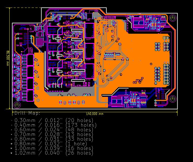
You can also find it in applications such as computers, data storage, file servers, cell phone transmitters and repeaters.
Other applications include weather analysis equipment, atomic accelerators, equipment for a space probe, and the fire alarm control system.
The advantages of using it include smaller size, high assembly density, increase in flexibility, easy incorporation and reduction in interconnections.
4.High-Speed PCB Design
A high-speed PCB design is any type of printed circuit board that involves the interruption of the equipment signals.
The interruption of the signals is by physical characteristics of the circuit board such as packaging, layout and interconnections.
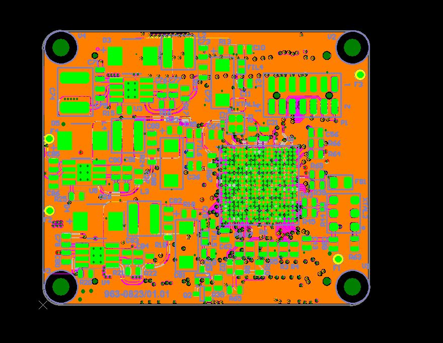
It involves issues such as reflection crosstalk, delays or emissions whenever you initiate the designing of the boards.
It is one of the most distinct designs due to the kind of attention it receives. You can use one to design a board where the main focus is on component routing and placement.
With designs of high speed, it is important to:
- Know the exact place for putting the traces
- Know how close the traces are to the signals
- Note the exact nature of the items you will connect.
Such considerations are important for taking the design to a new level of functionality.
5.High Power PCB Design
The most significant rule that you should look at is knowing the power path of the printed circuit board.
The amount of power and the location of the circuit is another significant consideration to focus on high power PCB designs.
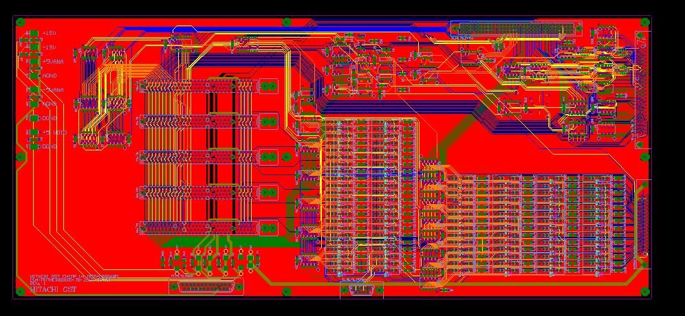
Apart from these factors, there are other factors to consider in high power PCB designs which include:
- The quantity of power that flows through the circuit
- Ambient temperature resulting around the board and the design
- The quantity of airflow around the board and the device
- The material you will use in making the board
- The density of the IC on the board
You will use this type of printed circuit board in devices that require the use of high power.
Since devices are becoming smaller and smaller by the day, PCB designs should be high power tolerant.
6. HDI PCB Design
High-Density Interconnect printed circuit boards is one of the fastest growing technologies for the PCB designs.
HDI PCB’s contain buried and/or blind vias and microvias that are less than a diameter thick usually 0.006 micrometres.
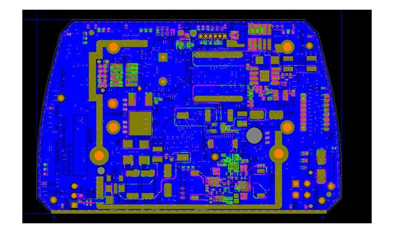
The circuitry density of this board is higher than the normal densities of the printed circuit boards.
High-Density Interconnect boards are available in six different types which include:
- The through vias extending from one surface to another surface
- A board with both buried and through vias
- Multilayer high density interconnect that have through vias
- Passive substrates that do not have any electrical connections
- Coreless construction of the HDI printed circuit boards using layer pairs
- An alternate construction of the HDI printed circuit boards using layer pairs
The benefits of using this type of printed circuit board include:
- It gives an allowance for placing more components on the two sides of the printed circuit board
- The multiple via process available allow the manufacturer to place smaller components very close to other components
- The decrease in pitch and size of the components allow for an increase in I/O in geometries of smaller sizes
- Allows for fast transmission of signals and reduces crossing delays and signal loss significantly.
7. LED PCB Design
Light Emitting Diode printed circuit board is an advancement in technology for the LED lighting. It features the connection of the LED to the circuit board and a chip producing light whenever the electric current flows.
Bonding of the chips is possible through the use of ceramic bases and thermal heat sinks.
The heat it generates is very high thus cooling through traditional means is very difficult.
You will, therefore, find metal cores in LED PCB’s because of the ability to release heat.
The most common piece of metal you will find in the LED PCB is aluminium.
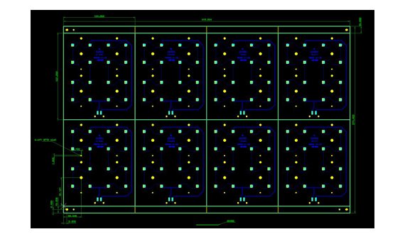
An aluminium PCB will include a thin layer of dielectric material that is able to conduct enough heat.
It is able to conduct and transfer heat from the system making it better than the traditionally printed circuit boards.
You will find the LED PCB design in different applications due to the following excellent abilities:
- It is energy efficient
- It is cost effective and you will save a lot for this type of design
- The design offers for maximum flexibility when you are using it
The applications that require the LED PCB include automotive headlights, military lighting applications, airport runway lighting, and street lighting.
Other applications are lighting in the highway tunnels, photovoltaic or solar lighting, lanterns and flashlights, signals and traffic lightings.
You may also find it in hospital lightings such as the theatre or operating rooms and growing plant lightings among others.
8. RF PCB Design
Radiofrequency printed circuit board designs is one of the most exciting pieces’ engineers have been working on.
You are likely to find the high-frequency boards in the upcoming technological inventions such as smartphones, robotics and sensors.
The high complexity of the design makes it an extremely difficult design to come up with.
The Industry of the printed circuit boards will consider any PCB operating above 100MHz as a radio frequency PCB.
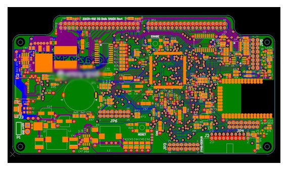
The devices that use the RF PCBs are complex and can accommodate both analog and digital signals.
There are certain devices that can accommodate different configurations of 60 layers.
9. High Voltage PCB Design
The high voltage printed circuit board design is common in different applications that require very high voltages.
It is important to have enough space and suitable clearances when designing the high voltage printed circuit board.
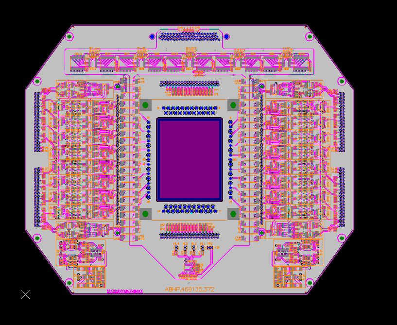
It helps in the elimination of any electrical breakdowns or electrical arcing.
When you are planning to come up with the high voltage PCB, there are certain considerations to look at.
The considerations include altitude, clearance, creepage distance, double insulation, reinforced insulation, basic insulation, supplementary insulation, and functional insulation.
The grade of insulating material, the altitude, environment, and type of PCB affect the creepage and clearance.
10. Amplifier PCB Design
You are most likely to find amplifier PCB designs in devices that produce sound with low to high-frequency audio devices.
The aspects of designing a complete functional audio circuit have been a challenge since it is very complex.
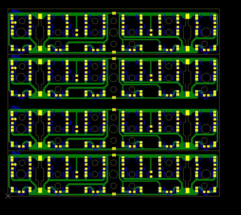
It is therefore important to have a specific layout that you will follow during the designing process.
The factors to consider when designing an amplifier PCB design are:
- The power supply and the grounds for power supply where transformers are the best
- Signals where you will avoid the in and out signals flowing to and from the IC
- Interfacing should be according to the design layout of the particular amplifier PCB design
- Capacitors where the audio signals will be passing through
- Op Amp circuits which will help in inverting of audio signals to achieve simple circuits
11. Metal Core PCB Design
Metalcore printed circuit boards or MCPCB are boards that use metal as the base material to spread the heat.
The base metals come as alternatives for CEM3 or FR4 boards as it disseminates heat faster and better.
Metal core will spread the heat to other fewer heat areas such as the metallic core or heatsink backing.
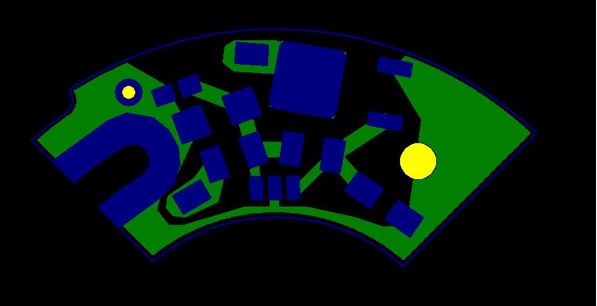
The type of metal material you can use in making the metal core printed circuit board will vary accordingly.
The most common metal materials are aluminium, copper or different mixtures of metal alloys. Again, the thickness of the metal core should range from 30 mils to 125 mils even though the thickness varies.
The advantages of using the metal core printed circuit board are as follows:
- It has the ability to integrate dielectric polymer layers that have high thermal conductivity for low thermal resistance
- It transfers heat 8 to 9 times faster in comparison to other materials such as the FR4
- It also laminates decapitate heat and keeps the heat generating components cool thus increased performance and longevity of life
// Frequently Asked Questions (FAQ)PCB layout & design (FAQ)
PCB layout design is the process of arranging and connecting electronic components on a printed circuit board to create a functional circuit. It starts with schematic capture, followed by strategic component placement and routing of conductive pathways. Designers consider electrical performance, manufacturability, and assembly requirements, applying design rules and DFM/DFA guidelines. The process includes simulations and prototype testing to ensure reliability. The final design is translated into manufacturing files, such as Gerber files, for PCB fabrication and assembly.
PCB designs come in various types to meet different application needs, including single-sided, double-sided, and multi-layer PCBs for varying complexity levels. Specialized types include rigid PCBs for durability, flexible and rigid-flex PCBs for space-constrained applications, high-frequency PCBs for RF and microwave use, aluminum-backed PCBs for superior heat dissipation, HDI PCBs for high-density component placement, and embedded PCBs for integrating components into the substrate. Each type is tailored to specific requirements, ensuring optimal performance, durability, and manufacturability across a wide range of electronics.
The cost of PCB design is calculated based on board complexity, material selection, design features, manufacturing requirements, design services, and regulatory compliance. Factors such as the number of layers, substrate material, component density, HDI features, impedance control, special finishes, prototype vs. production runs, turnaround time, testing, labor, expertise, and compliance standards all contribute to the overall cost. Understanding these elements helps in budgeting and optimizing the design process for cost-effectiveness.
PCB design is integral to numerous industries, including consumer electronics, automotive, telecommunications, medical devices, industrial automation, aerospace and defense, computing, energy and power, and instrumentation and measurement. Each industry relies on PCB technology to develop sophisticated, reliable, and efficient electronic products and systems. The versatility and critical nature of PCBs make them indispensable across a broad spectrum of applications, driving innovation and functionality in modern technology.
Selecting a PCB design software manufacturer involves evaluating functionality and features, ease of use, compatibility and integration, performance and reliability, support and community, cost and licensing, scalability, reputation and reviews, industry-specific requirements, and trial and evaluation options. Carefully considering these factors will help you choose software that enhances your design capabilities, fits your budget, and supports your long-term needs.
Effective PCB layout design requires adherence to design rule checks, signal integrity principles, power distribution techniques, thermal management, and manufacturability guidelines. Proper component placement, layer stack-up, and testing considerations are crucial for creating reliable and functional PCBs. Following these rules helps ensure the final PCB design is manufacturable, performs well, and meets industry standards and regulatory requirements.
The high-speed PCB design process requires a meticulous approach to handle the complexities of high-frequency signal transmission. It involves careful schematic design, precise PCB layout, signal integrity analysis, thermal and EMC considerations, and thorough testing. By following these steps, designers can create PCBs that perform reliably and efficiently in high-speed applications, ensuring optimal signal integrity and overall system performance.
