PCB Surface Finishes

Compare PCB surface finishes including ENIG, Lead-Free HASL, OSP, Immersion Silver, Immersion Tin, Hard Gold and ENEPIG for solderability, reliability and cost.

PCB FABRICATION · GLOBAL SUPPLY

Engineered PCB Surface Finishes

Reliable solderability, controlled metal thickness and application-specific protection—from standard lead-free finishes to ENEPIG and nickel-free EPIG.

Prototype to VolumeMixed & Selective FinishesEngineering Review

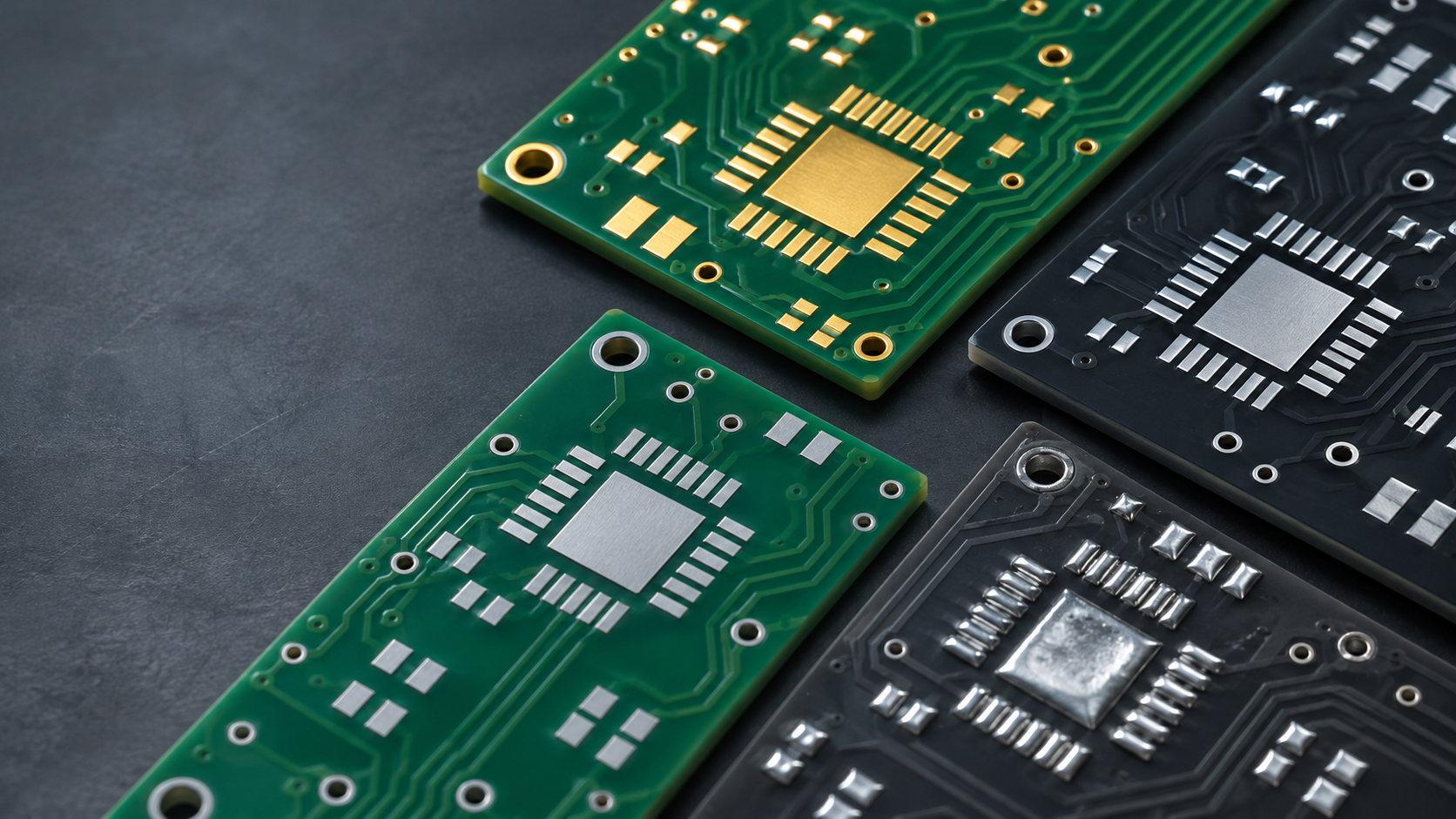
PCB surface finish comparison with gold silver and tin pads

14+finish configurations
EPIG capabilityPd 1–5 µin · Au 1–5 µin
520 × 800 mmMaximum listed ENIG size
3 milPrototype ENIG pad-to-trace gap
0.2–7.0 mmListed ENIG board thickness
DFM + CAM ReviewFinish stack checked before release

Surface Protection and Solderability

Why PCB Surface Finish Matters

A PCB surface finish protects exposed copper from oxidation and creates a dependable surface for component soldering, wire bonding, edge connectors and electrical contact. The correct finish depends on component pitch, assembly process, operating environment, storage requirements, production volume and target cost.

KKPCB reviews your PCB design and application requirements to help select a finish that balances solderability, surface flatness, durability and manufacturing cost.

Close-up comparison of gold, silver and tin PCB surface finishes

Different finishes create visibly different pad surfaces, but selection must be based on assembly and reliability requirements—not appearance alone.

Finish Function at a Glance

One PCB, Several Possible Interfaces

A surface finish is the controlled interface between bare copper and the next manufacturing step. It influences wetting, pad coplanarity, contact resistance, wire-bond compatibility, storage behavior and the risk profile of repeated thermal cycles.

For fine-pitch assembly: prioritize flatness and consistent pad geometry.
For repeated contact: prioritize wear resistance and stable electrical contact.
For RF or bonding: review the metal stack, nickel layer and bonding method together.
For storage: control packaging, humidity, contamination and time to assembly.

Available Processes

PCB Surface Finish Options

From cost-effective standard finishes to advanced finishes for fine-pitch components and wire bonding, our manufacturing options cover a wide range of PCB applications.

01 / STANDARD

Lead-Free HASL

A cost-effective lead-free finish with excellent solderability for conventional through-hole and SMT assemblies where extreme pad flatness is not required.

Best for: Industrial controls, power electronics and standard PCB assemblies.

02 / FLAT & RELIABLE

ENIG

Electroless Nickel Immersion Gold provides a flat, oxidation-resistant surface suitable for fine-pitch SMT, BGA, QFN and high-density PCB designs.

Best for: BGA, QFN, fine-pitch SMT and high-density boards.

03 / COST-EFFICIENT

OSP

Organic Solderability Preservative creates a thin protective coating directly over copper and offers excellent surface flatness for lead-free assembly.

Best for: Fine-pitch SMT and cost-sensitive volume production.

04 / LOW RESISTANCE

Immersion Silver

A flat, solderable surface with low contact resistance, suitable for fine-pitch assembly and selected high-frequency applications.

Best for: RF boards, communication equipment and fine-pitch components.

05 / PRESS-FIT

Immersion Tin

A flat, lead-free surface supporting SMT, press-fit connections and applications requiring consistent pad geometry.

Best for: Press-fit connectors, automotive electronics and SMT assemblies.

06 / WEAR RESISTANT

Hard Gold

Electroplated Hard Gold provides high wear resistance and stable electrical contact performance on repeated-contact areas.

Best for: Gold fingers, edge connectors, keypads and test contacts.

07 / ADVANCED

ENEPIG

Electroless Nickel Electroless Palladium Immersion Gold supports soldering and selected wire-bonding requirements for complex assemblies.

Best for: Wire bonding, advanced packaging and high-reliability electronics.

08 / NICKEL-FREE

EPIG

Electroless Palladium Immersion Gold is a nickel-free Pd/Au system. KKPCB supports Pd 1–5 µin and Au 1–5 µin (each approximately 0.025–0.127 µm) for reviewed bonding, fine-pitch and RF requirements.

Best for: Nickel-sensitive designs, selected wire bonding, fine-pitch and RF applications.

Verified Factory Capability

KKPCB Surface Finish Production Capability

The following limits combine KKPCB’s released production capability sheet with current process confirmation. Prototype and small-to-medium volume limits are shown separately where released values differ. Final manufacturability remains subject to board construction, panel utilization and engineering review.

14+listed finish and mixed-finish configurations
520 × 800 mmmaximum listed ENIG finishing size
0.2–7.0 mmlisted PCB thickness range for ENIG
3 milprototype ENIG pad-to-trace minimum

01

Supported Finish Configurations

Regular and mixed-finish options listed in the KKPCB capability sheet.

Lead-Free HASLHASL*ENIGENEPIGEPIGImmersion Silver (ImAg)Immersion Tin (ImSn)OSPPlated Hard GoldENIG + OSPLead-Free HASL + Gold FingersENIG + Gold FingersFlash Gold + Selective Hard GoldOSP + Gold Fingers

*Leaded HASL is listed in the source capability sheet but requires customer, regulatory and destination-market review.

02

Board Size and Thickness Windows

Use these values for early RFQ screening. Line-specific limits still require CAM confirmation.

Finish Maximum finishing size Minimum finishing size PCB thickness range
ENIG 520 × 800 mm Confirm by panelization 0.2–7.0 mm
Immersion Tin Vertical: 500 × 600 mm
Horizontal: single dimension <500 mm
60 × 80 mm 0.3–7.0 mm; line-specific review applies
Immersion Silver Horizontal: single dimension <500 mm 60 × 80 mm 0.3–3.0 mm
HASL / Lead-Free HASL 520 × 650 mm 150 × 230 mm 0.6–3.5 mm; thin boards require review
OSP Single dimension <500 mm 60 × 80 mm 0.3–3.0 mm
Plated Gold Hard gold: 450 × 500 mm; single dimension up to 520 mm Confirm by tooling and plating layout 0.3–5.0 mm; listed thickness ratio 10:1

03

Finish Thickness Capability

Original microinch values are retained, with metric conversions added for quotation clarity.

Finish Prototype capability Small / medium volume capability RFQ note
HASL 1–40 µm 1–40 µm Specify lead-free or SnPb and applicable compliance.
ENIG Ni 3–6 µm; Au 1–5 µin (0.025–0.127 µm) Ni 3–6 µm; Au 1–4 µin (0.025–0.102 µm) Gold above 5 µin requires engineering review.
Immersion Tin ≥1 µm ≥1 µm Confirm storage and assembly timing.
Immersion Silver 6–12 µin (0.152–0.305 µm) 6–12 µin (0.152–0.305 µm) Define packaging and tarnish-control requirements.
OSP 0.2–0.4 µm 0.2–0.4 µm Confirm reflow count and handling controls.
ENEPIG Ni 3–5 µm; Pd 1–6 µin; Au 1–4 µin Ni 3–5 µm; Pd 1–6 µin; Au 1–4 µin State soldering and wire-bond requirements.
EPIG Pd 1–5 µin (0.025–0.127 µm); Au 1–5 µin (0.025–0.127 µm) Pd 1–5 µin (0.025–0.127 µm); Au 1–5 µin (0.025–0.127 µm) Nickel-free capability; define bonding, RF and acceptance requirements.
Plated Hard Gold 2–80 µin (0.051–2.032 µm) 2–50 µin standard; thicker deposits require review Specify hardness, contact area and wear requirement.
Selective Plated Gold 2–80 µin; dense features may require review 2–50 µin standard; thicker deposits require review Identify local area and provide plating-bar design.
Gold Fingers 2–80 µin 2–80 µin Confirm bevel angle, nickel thickness and mating cycles.

04

Minimum Feature Rules

ENIG IC / pad-to-trace gapPrototype: 3 mil
Small / medium volume: 4 mil
Gold-finger gapPrototype: 5 mil
Small / medium volume: 6 mil
Gold-finger bevel angles20°, 30°, 45° and 60° listed
Angle tolerance: ±5°
Finger-to-outline spacingMinimum listed distance: 8 mil

05

Specify These Items on the RFQ

  • Finish name and chemical or electrolytic deposition method.
  • Metal stack and minimum / nominal thickness for each layer.
  • Whole-board, local or mixed-finish treatment area.
  • Prototype or volume-production requirement.
  • Gold-finger bevel, hardness and mating-cycle requirement.
  • RoHS status, storage life, soldering profile and test requirement.
Capability boundary: values above describe KKPCB’s released process capability sheet, not a universal guarantee for every PCB. Stack-up, aspect ratio, panelization, copper distribution, selective-plating layout and customer acceptance criteria may change the manufacturable window.

Finish-by-Finish Engineering Guide

Advantages, Limitations and Best-Fit Applications

The following summaries turn the supplied comparison material into practical design guidance. Final availability, thickness and acceptance criteria must be stated on the fabrication drawing.

Lead-Free HASL SnCuNi

Molten lead-free solder coats exposed copper and is leveled with hot air. It remains a robust, economical choice for conventional PCB assembly.

Advantages

Strong solderability, broad process familiarity, good visual coverage and a comparatively low process-cost index.

Limitations

Less planar than chemical finishes; not preferred for very small BGA/QFN pads or demanding coplanarity.

ENIG Ni / Au

Electroless nickel forms the barrier layer and immersion gold protects the nickel until soldering. The result is flat and oxidation resistant.

Advantages

Excellent flatness for BGA and fine-pitch SMT, stable handling and a well-established high-density finish.

Limitations

Higher cost than HASL/OSP; nickel and gold deposition must be tightly controlled to prevent interface defects.

OSP Organic on Cu

A very thin organic film protects copper directly and is removed during soldering, leaving a copper-to-solder joint.

Advantages

Very flat, economical, lead-free and suitable for fine-pitch pads when assembly is well controlled.

Limitations

Sensitive to handling, abrasion and heat history; the source comparison limits multiple soldering to 1–2 cycles.

Immersion Silver Ag

A thin, planar silver layer protects copper and provides low contact resistance with strong solderability.

Advantages

Fine-pitch friendly, suitable for selected high-frequency designs and capable of multiple reflow cycles when protected.

Limitations

Fingerprints, sulfur, chlorides and poor packaging can cause tarnish or contamination; disciplined handling is essential.

Immersion Tin Sn

A planar tin coating supports fine-pitch SMT and press-fit applications while maintaining consistent pad geometry.

Advantages

Flat, lead-free, solderable and compatible with press-fit designs; refreshable in the supplied process matrix.

Limitations

Oxidation and intermetallic growth make storage and assembly timing important; not a general-purpose long-storage finish.

ENEPIG Ni / Pd / Au

A palladium layer between nickel and gold supports soldering plus selected aluminium- and gold-wire bonding requirements.

Advantages

Versatile for mixed assembly/bonding, fine-pitch work and high-reliability electronics.

Limitations

More complex and more expensive than ENIG; the complete metal stack must match the bonding and soldering process.

EPIG — Nickel-Free Palladium Gold Pd / Au

EPIG omits the nickel barrier and uses electroless palladium with gold. It is distinct from ENIPIG, which still contains nickel.

Advantages

KKPCB supports Pd 1–5 µin and Au 1–5 µin (each approximately 0.025–0.127 µm) for nickel-sensitive RF paths, fine pitch, soldering and selected wire-bonding applications.

Limitations

Confirmed thickness capability still requires drawing review, defined acceptance criteria and application qualification.

Electroplated Gold Hard / Soft Au

Electrical current deposits gold over nickel. Hard gold is optimized for wear contacts; soft gold is selected for bonding or specialized interconnects.

Advantages

Hard gold withstands repeated mating; soft gold supports application-specific wire bonding and high-reliability contacts.

Limitations

Requires plating connections and selective design planning; hard gold is not the default solderable pad finish.

Gold Finish Selection

ENIG vs Electroplated Gold: They Serve Different Functions

The supplied gold-process notes correctly distinguish chemical immersion gold from electrolytic plating. The engineering decision is based on function, not simply the color of the finished board.

ENIG / Chemical Gold

  • Deposited chemically after solder mask over exposed copper pads.
  • Flat surface for soldering, BGA, QFN and fine-pitch SMT.
  • Thin immersion-gold protection over an electroless-nickel barrier.
  • Choose when pad coplanarity and assembly performance are primary.

Electroplated Hard or Soft Gold

  • Requires an electrical plating path and is commonly selective.
  • Hard gold is used for gold fingers, key contacts and repeated mating.
  • Soft gold is used for selected wire-bonding/interconnect functions.
  • Choose when wear life, contact function or bonding drives the requirement.
ENIGPlanar • typical source shelf reference: 24 months
Electroplated GoldPlanar • wear/contact focused • source reference: 24 months
OSPPlanar • lowest source cost index • source reference: 6 months
Immersion SilverPlanar • low resistance • source reference: 12 months
Immersion TinPlanar • press-fit friendly • source reference: 6 months
HASLLess planar • strong solderability • source reference: 18 months

Shelf-life values above reproduce the supplied legacy comparison chart for context only. They are not guaranteed storage limits; actual shelf life depends on the approved finish, packaging, environment and customer specification.

Complete Coating Reference

Surface Finish Layer Structures and Thicknesses

The following reference structures are taken from the supplied Surface Finish Overview. They are engineering starting points; the final stack and thickness must be confirmed on the approved fabrication drawing.

ENAGNi: 3-7 µmAu: 0.1-0.3 µmElectroless NiElectroless Au
ENIGNi: 3-7 µmAu: 0.05-0.125 µmElectroless NiImmersion Au
ENEPIGNi: 3-7 µmPd: 0.05-0.3 µmAu: 0.04-0.1 µm
ENIPIGNi: 3-7 µmPd: 0.01-0.05 µmAu: 0.04-0.1 µm
EPPd: 0.1-0.2 µmNickel-freePalladium only
EPAGPd: 0.1-0.2 µmAu: 0.1-0.2 µmNickel-free
EPIG – Nickel-Free Palladium GoldPd: 1–5 µin (0.025–0.127 µm)Au: 1–5 µin (0.025–0.127 µm)KKPCB capability · Nickel-free
Electroplated Hard GoldNi: >4 µmAu: 0.8-3 µmWear contacts
Electroplated Soft GoldNi: >4 µmAu: 0.2-0.5 µmBonding
Lead-Free HASLSnCuNi alloy: 1-50 µmRefreshable
Lead-Containing HASLSnPb alloy: 1-50 µmLegacy / compliance review
Immersion SilverAg: 0.2-0.4 µmFlat surface
ISIGAg: 0.2-0.3 µmAu: 0.04-0.15 µm
Immersion TinSn: 0.8-1.3 µmRefreshable
OSPOrganic coating: 0.2-0.6 µmRefreshable
Important: Lead-containing HASL appears in the source matrix for comparison. Production availability is project-specific and subject to RoHS, customer and destination-market requirements.

Detailed Engineering Matrix

Compare Assembly, Bonding and Reliability Performance

This expanded matrix converts the source document’s symbols into plain-language ratings for web use. Use it for early selection, then confirm the finish against the assembly profile, component geometry and reliability target.

RecommendedGoodWith limitationsNot recommended / unsuitable
Finish Soldering Multiple Soldering Fine Pitch <75 µm Al-Wire Au-Wire High Frequency Press-Fit Key / Contact Corrosion Shelf Life Refreshable Source Cost Index
ENIG 3x With limitations Not recommended With limitations With limitations Good With limitations No 100%
ENEPIG 3x With limitations With limitations With limitations Good No 120%
ENIPIG 3x With limitations Good With limitations With limitations Good No 115%
EPIG 3x Good Good No 125%
Hard Gold With limitations No Not recommended Unsuitable Unsuitable With limitations With limitations No Local / selective
Soft Gold Good No Not recommended Good With limitations With limitations No >200%
Lead-Free HASL Good 3x Not recommended Unsuitable Unsuitable With limitations Not recommended Yes 70%
Immersion Silver 3x Good Not recommended With limitations Not recommended With limitations With limitations No 50%
ISIG 3x With limitations Not recommended With limitations No 125%
Immersion Tin 3x Unsuitable Unsuitable With limitations Unsuitable With limitations Yes 60%
OSP Good 1-2x Unsuitable Unsuitable Good Not recommended With limitations Not recommended With limitations Yes 30%

Cost indexes are relative values from the supplied comparison sheet, where ENIG is shown as 100%. They are not quotations. Actual price depends on board area, selective plating, thickness, volume and compliance requirements.

Complete Source Matrix

All 16 Surface Finish Systems in the Supplied Overview

The following table preserves every process designation, description, remark, layer-thickness value, multiple-soldering figure, refreshability indication, relative cost index and chemistry reference stated in the supplied surface-finish overview. Dashes indicate that the source does not state a value.

SolderingMultiple solderabilityAl wire bondingAu wire bondingFine pitch <75 µmHigh frequencyPress-fitKey contactsCorrosion resistanceShelf lifeRefreshabilityLong-term / market references
Code Full process Source remarks Layer structure / nominal thickness Multiple solderability Refreshable Relative cost Chemistry references in source
ASIG Electroless Silver / Immersion Gold Semireductive gold. The reductive silver bath is described as unstable and the process has largely been replaced by ISIG. Ag + Au (thickness not stated in the source) — No — —
ENAG Electroless Nickel / Electroless Gold Phosphorous nickel; reductive gold chemistry is described as unstable and increasingly replaced by palladium alternatives. Ni 3–7 µm; Au 0.10–0.30 µm 2× No 140% Umicore
ENEPIG Electroless Nickel / Electroless Palladium / Immersion Gold Phosphorous nickel and palladium. A higher gold thickness can be produced with semireductive gold deposition. Ni 3–7 µm; Pd 0.05–0.30 µm; Au 0.04–0.10 µm 3× No 120% Atotech; Umicore (TRG)
ENIG Electroless Nickel / Immersion Gold Phosphorous nickel; established flat solderable finish for fine-pitch assembly. Ni 3–7 µm; Au 0.05–0.125 µm 3× No 100% reference OMG; Atotech; Umicore
ENIPIG Electroless Nickel / Immersion Palladium / Immersion Gold Phosphorous nickel and palladium. Higher gold thickness is possible when required. Ni 3–7 µm; Pd 0.01–0.05 µm; Au 0.04–0.10 µm 3× No 115% OMG; Umicore (TRG)
EP Electroless Palladium Palladium layer without phosphorus. Pd 0.10–0.20 µm 3× No 90% Atotech (Pallabond); Umicore
EPAG Electroless Palladium / Electroless Gold Palladium without phosphorus combined with semireductive gold. Pd 0.10–0.20 µm; Au 0.10–0.20 µm 3× No 125% Atotech (Pallabond)
EPIG Electroless Palladium / Semireductive Gold Palladium without phosphorus; intended for specialized bonding and functional applications. Pd 0.10–0.20 µm; Au 0.04–0.20 µm 3× No 125% Umicore (TRG)
GalvNiG hard Electroplated Nickel / Hard Gold Cobalt- or iron-doped gold bath. Nickel hardness 400–450 HV; gold hardness 140–170 HV. Ni >4 µm; Au 0.8–3.0 µm No No Local spots / selective Dow; Atotech; Umicore
GalvNiG soft Electroplated Nickel / Soft Gold Fine-gold electrolytes for bonding and soldering. Nickel hardness 400–450 HV; gold hardness 80–110 HV. Ni >4 µm; Au 0.20–0.50 µm No No >200% Dow; Atotech; Umicore
HAL lead free Lead-Free Hot Air Solder Leveling Also commonly called HAL or HASL; SnCuNi alloy coating. SnCuNi alloy 1–50 µm 3× Yes 70% Balver Zinn; Felder Lote
HAL lead containing Leaded Hot Air Solder Leveling Also commonly called HAL or HASL; SnPb alloy coating. SnPb alloy 1–50 µm 3× Yes 70% Balver Zinn; Felder Lote
IS Immersion Silver Thin, planar silver finish. Handling and packaging control are essential to avoid tarnish and contamination. Ag 0.20–0.40 µm 3× No 50% MacDermid; Umicore
ISIG Immersion Silver / Immersion Gold Silver followed by semireductive gold. Ag 0.20–0.30 µm; Au 0.04–0.15 µm 3× No 125% Umicore (TRG)
IT Immersion Tin Planar tin finish; susceptible to oxidation and requires controlled storage and assembly planning. Sn 0.80–1.30 µm 3× Yes 60% Atotech (Smarttin)
OSP Organic Solderability Preservative Organic surface passivation over copper; economical and flat, but process and handling limits apply. Organic coating 0.20–0.60 µm 1–2× Yes 30% Enthone (Entek+HT)

The percentages are relative process-cost indices from the supplied comparison material, with ENIG defined as 100%; they are not sales quotations or guaranteed production pricing. Supplier names are chemistry references appearing in the source, not endorsements.

Complete Process Map

Complete PCB Surface Finish Classification

PCB finishes should not be compared as one flat list. A practical engineering classification separates solderable final finishes, electrolytic metal systems, selective or composite processes, and functional conductive coatings. Names that describe the same chemistry are not counted twice.

01

Solderable Final Finishes

Protect exposed copper and provide a reliable surface for component assembly.

Leaded HASLHASLLegacy SnPb hot-air solder leveling; compliance review required.
Lead-Free HASLLF-HASLEconomical Sn-based hot-air leveling for standard assembly.
Organic Solderability PreservativeOSPVery flat organic protection directly over copper.
Immersion SilverImAg / ISFlat, low-resistance silver for soldering and selected RF use.
Immersion TinImSnFlat tin finish for SMT and selected press-fit designs.
Electroless Nickel Immersion GoldENIGNickel barrier plus immersion gold for flat fine-pitch assembly.
Electroless Nickel Electroless Palladium Immersion GoldENEPIGNi/Pd/Au stack for soldering and selected bonding requirements.

02

Electrolytic Metal Finishes

Used where controlled metal thickness, wear, conductivity or contact reliability is required.

Electrolytic Hard GoldHard AuGold fingers, edge connectors, key contacts and repeated mating.
Electrolytic Soft GoldSoft AuApplication-specific wire bonding and high-reliability interconnects.
Electrolytic Nickel / GoldNi/AuContact pads and special functional areas; hardness must be specified.
Electrolytic Gold PlatingAu PlateGeneral term; gold purity, hardness and thickness require definition.
Electrolytic SilverAg PlateSpecial high-conductivity or functional contact regions.
Electrolytic TinSn PlateSpecial solderable or protective use.
Electrolytic Tin-LeadSnPb PlateTraditional process; regulatory and destination-market review required.

03

Composite, Nickel-Free & Selective Systems

Special stacks or local processing where different PCB areas require different functions.

ENEPIGNi / Pd / AuAlso appears in solderable finishes because it serves both assembly and bonding; it is one process, not two.
EPIGPd / AuNickel-free palladium/gold system; distinct from ENEPIG.
ENIG + Selective Hard GoldMixedENIG solder pads with hard-gold fingers or contact zones.
Selective ENIGLocal ENIGENIG applied only to designated areas.
Selective Gold PlatingLocal AuElectrolytic gold on specified functional regions.

04

Functional Conductive Coatings

Conductive inks and local coatings are functional treatments, not equivalent to standard solder-pad finishes.

Carbon InkCarbonKeypads, switch contacts and cost-controlled conductive areas.
Silver PasteAg PastePrinted conductive traces and special interconnect features.
Conductive Carbon CoatingC CoatingContact and conductive regions requiring a carbon interface.
Selective Immersion SilverLocal ImAgImmersion silver only on specified soldering or RF areas.
Selective Immersion TinLocal ImSnImmersion tin only on designated solderable areas.
Counting rule: the industry has roughly 8–10 mainstream commercial finish families. A list can exceed 20 names when it includes electroplating variants, selective combinations and functional coatings, but aliases and repeated process names must not be counted as separate finishes.

RFQ Name Control

Names That Must Be Clarified Before Quotation

Customer drawings often use abbreviated or generic wording. Engineering must confirm the actual deposition method, metal stack, hardness, thickness and treated area.

Ni/Au or Au/NiGeneric nickel/gold wording—confirm electroless versus electrolytic and layer order.
Immersion GoldUsually refers to the immersion-gold step in ENIG; confirm whether a nickel barrier is required.
Flash GoldUsually a thin gold deposit; confirm plating method, purity and minimum thickness.
Selective GoldDefines local treatment, not the gold chemistry; confirm hard, soft, ENIG or another stack.
White TinDescriptive tin wording; confirm immersion tin, electrolytic tin or solder coating.
Tin PlatingConfirm whether the requirement is electrolytic tin or chemical immersion tin.
ImAgCommon abbreviation for Immersion Silver.
ImSnCommon abbreviation for Immersion Tin.
Bare Copper / Pre-fluxMay appear in special process notes but should not be treated as a standard finished-board surface finish.

KKPCB Standard RFQ Taxonomy

HASLLead-Free HASLOSPENIGENEPIGImmersion SilverImmersion TinHard GoldSoft GoldElectrolytic Ni/AuElectrolytic SilverElectrolytic TinElectrolytic SnPbEPIGSelective GoldCarbon InkSilver Paste

Five Items to Confirm on Every RFQ

  • Required gold, nickel, palladium, tin or silver thickness.
  • Chemical deposition or electrolytic plating.
  • Whole-board finish or selective/local treatment.
  • Gold-finger hardness and beveling requirement.
  • RoHS status, soldering profile, storage life and reliability target.

This classification supports sales, quotation and engineering review. It does not state that every listed process is available for every construction. Final capability, thickness window and acceptance criteria remain subject to KKPCB engineering review and the released fabrication drawing.

Handling Is Part of the Finish

Protect the Surface After Plating

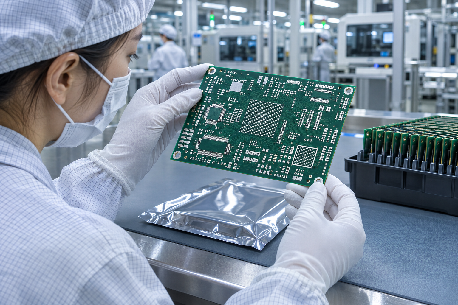
The most capable finish can still fail if it is touched, contaminated, exposed to sulfur/chlorides or stored in unsuitable packaging. Clean gloves, controlled drying, approved interleaving materials and sealed packaging preserve solderability until assembly.

Handle boards by the edges with clean, dry gloves.
Keep silver away from sulfur-, chloride- and acid-bearing materials.
Reseal opened packages and minimize delay before assembly.

Technician inspecting a finished PCB with clean gloves before packaging

Process Control & Handling

From Chemical Preparation to Assembly Storage

Surface-finish quality depends on the entire chain: copper preparation, controlled deposition, rinsing and drying, packaging, storage and assembly discipline.

Typical Precious-Metal Process Control

  1. Clean and condition the copper surface; remove oils, oxides and residues.
  2. Microetch to create a fresh, uniform copper surface, followed by thorough rinsing.
  3. Activate the surface and deposit the specified nickel, palladium, silver or gold layers in the defined sequence.
  4. Control bath condition, temperature, dwell time, loading and agitation; verify thickness and appearance.
  5. Use clean final rinses and complete drying before inspection and packaging.

Immersion Tin — Reference Process Sequence

The supplied CSN Classic material describes the following general route:

CleanerRinseMicroetchRinsePredipImmersion TinWarm RinseDI RinseDry
  • Cleaner: 10–15 vol%, 40–50°C, 1–3 min.
  • Microetch: approximately 2%, 28–42°C, about 2 min; typical copper removal 1–2 µm.
  • Predip: 15–30°C, less than 1 min.
  • Tin bath: 63–73°C horizontal or 56–65°C vertical; typical dwell 7–11 or 9–15 min.
  • Warm rinse 50–60°C, followed by a 50°C DI rinse.

These are reference values from supplied chemistry literature. Production parameters must follow the approved chemical supplier specification and KKPCB process control plan.

Immersion Silver — Performance

  • Planar finish with consistent solderability and low contact resistance.
  • Supports multiple reflow cycles and can be suitable for aluminium-wire bonding when correctly specified.
  • Offers good solder-joint strength, touch-contact functionality and a comparatively simple process route.
  • Long shelf life and tarnish resistance depend on correct production, handling and packaging.

Immersion Silver — Handling & Storage

  • Always use clean, dry gloves. Fingerprints, salts, acids and oils can cause tarnish and reduce solderability.
  • Routing before silver deposition is preferred. If routing follows plating, use sulfur- and acid-free interleaving material.
  • Clean only with DI water or electrostatic methods; avoid surfactant or acid cleaners. Use dedicated drying equipment.
  • Package promptly after cooling. Avoid chloride- and sulfide-bearing materials.
  • Store at no more than 30°C and 75% RH in sealed bags or containers; wrap first in sulfur-free paper so plastic does not touch the silver directly.
  • Keep desiccant away from direct board contact, positioned between plastic layers.
  • Do not use adhesive tape, labels, ink or rubber bands in direct packaging contact.
  • Properly produced and stored boards can retain properties for at least 12 months. After opening, rewrap and assemble promptly; an often-used mid-assembly guideline is about one week, subject to the actual environment.
  • If stress-relief baking is required, protect the boards with aluminium foil.

OSP Handling

  • Uniform copper cleaning and microetching are essential before organic passivation.
  • Avoid fingerprints, abrasion, excessive heat exposure and contamination after coating.
  • OSP is economical and very flat, but the supplied comparison limits multiple solderability to 1–2 cycles.
  • Use controlled storage and an assembly profile compatible with the selected OSP chemistry.

Inspection & Release

  • Confirm visual uniformity, coverage and absence of discoloration, stains or exposed base metal.
  • Verify thickness against the approved finish specification and drawing notes.
  • Where required, evaluate solderability, contact function, wire bonding, press-fit or corrosion performance using application-specific tests.
  • Packaging and labeling must preserve the finish through shipment and customer storage.

Fabrication Notes

Via Treatment Is Defined Separately from Surface Finish

Via covering, opening and plugging must follow the fabrication data and purchase requirements. The supplied process-comparison workbook adds the following practical rules:

Design Definition

  • The best result is obtained when via attributes are explicitly defined in the design and manufacturing follows the released files.
  • “According to design files” can result in vias being either exposed copper or covered by solder mask, depending on the actual data.
  • Via tenting normally means solder mask covers the via. If the requirement is plugging plus an opening, specify solder-mask plugging and the required opening clearly.

Engineering Review Rules

  • Ambiguous, partly exposed or conflicting via definitions require an engineering query before fabrication.
  • Vias larger than the validated plugging capability require engineering review.
  • A design with exposed copper on one side and solder mask on the other also requires review because appearance and quality can be affected.
  • Vias in BGA areas should be covered and plugged; other areas follow the released design. By default, BGA-area vias are treated as covered and plugged unless otherwise specified.

Immersion tin has a relatively short storage window and is sensitive to oxidation. The supplied workbook notes that it is generally not recommended for military products, where leaded HASL and immersion gold have historically been common choices; final selection must follow the customer drawing, applicable standards and regulatory requirements.

Specialized Processes

Advanced and Functional Finishes

This section separates confirmed KKPCB capability from processes that require drawing, thickness and application review. EPIG capability is confirmed; selective, electrolytic and functional coatings are evaluated against the RFQ.

Confirmed capability

EPIG — Nickel-Free Palladium Gold

Nickel-free palladium/gold stack for nickel-sensitive, selected RF and wire-bonding designs. Pd: 1–5 µin (0.025–0.127 µm); Au: 1–5 µin (0.025–0.127 µm).

RFQ review

ENEPIG

Electroless Nickel / Electroless Palladium / Immersion Gold for mixed soldering and wire-bonding requirements. This finish retains a nickel barrier.

RFQ review

ISIG

Immersion Silver followed by Immersion Gold for selected high-frequency, fine-pitch and bonding applications.

RFQ review

Electrolytic Soft Gold

High-purity soft gold for application-specific wire bonding and high-reliability interconnects.

RFQ review

Electrolytic Nickel / Gold

Controlled nickel and gold thickness for contact pads, connector areas and special functional surfaces.

RFQ review

Electrolytic Silver

Silver plating for special low-resistance conductive regions where the drawing defines thickness and protection requirements.

RFQ review

Electrolytic Tin

Electroplated tin for specified solderability or protection functions; do not confuse it with immersion tin.

RFQ review

Electrolytic Tin-Lead

Traditional tin-lead plating for legacy or exempt applications, subject to regulatory and customer requirements.

Selective combination

ENIG + Selective Hard Gold

ENIG on solderable pads combined with local hard gold on fingers or wear-resistant contacts.

Selective process

Selective Gold Plating

Electroplated gold only on drawing-defined areas, with gold type, nickel underplate and thickness clearly specified.

Selective process

Selective Immersion Silver

Local immersion silver on defined soldering or contact regions while other areas use a different finish.

Selective process

Selective Immersion Tin

Local immersion tin on drawing-defined solderable areas, with handling and storage controls confirmed before release.

Functional coating

Carbon Ink

Printed carbon for keypad contacts, switch pads and wear-resistant conductive surfaces.

Functional coating

Silver Paste

Printed silver conductive material for special circuit, shielding or interconnection functions.

Functional coating

Conductive Carbon Coating

Carbon-based conductive coating for defined contact or resistive areas; composition and resistance require review.

Terminology check

Flash Gold / Thin Gold

These are not complete process definitions. RFQs must state electroless or electrolytic deposition, underplate, purity and thickness.

Selection Workflow

Four Checks Before Releasing the Finish Specification

STEP 01Assembly MethodReflow count, wave soldering, hand soldering and repair requirements.
STEP 02Component GeometryBGA, QFN, fine-pitch pads, press-fit holes and connector layout.
STEP 03Electrical FunctionRF performance, contact resistance, wire bonding and repeated mating.
STEP 04Environment & StorageShelf life, corrosion exposure, handling and reliability targets.

Selection Guide

Which Surface Finish Should You Choose?

Our engineering team can review your Gerber files and assembly requirements before production.

Fine-Pitch Components

Choose ENIG, OSP, Immersion Silver or Immersion Tin for BGA, QFN and fine-pitch SMT components.

Cost-Sensitive Production

Lead-Free HASL and OSP are common choices when controlling production cost is a priority.

Connector Durability

Use Hard Gold for gold fingers, edge connectors and surfaces exposed to repeated mechanical contact.

Wire Bonding

Evaluate ENEPIG, nickel-free EPIG or application-specific electrolytic gold when the assembly requires wire bonding.

High-Reliability Products

ENIG and ENEPIG provide flat, durable surfaces for complex electronics, subject to application review.

RF and Communication Boards

Immersion Silver or other application-specific finishes can be considered for selected RF designs.

Controlled PCB Production

Consistent Finish Quality from Prototype to Production

Surface finish quality depends on controlled chemistry, process stability, coating thickness and proper handling. KKPCB applies documented manufacturing and inspection procedures to maintain consistent pad coverage, solderability and traceability.

Coating ControlControlled finish thickness according to approved specifications.
Solderability InspectionProcess verification for dependable assembly performance.
Surface InspectionAppearance and pad coverage inspection during production.
Microsection ReviewCross-section verification when required by the project.
Cleanliness ControlProduction handling and contamination-control procedures.
Lot TraceabilityManufacturing records from prototype through volume production.

Industry Applications

Surface Finishes for Diverse PCB Applications

Finish selection is matched to solderability, contact wear, corrosion exposure, signal integrity and assembly requirements in each application.

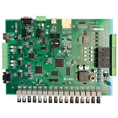
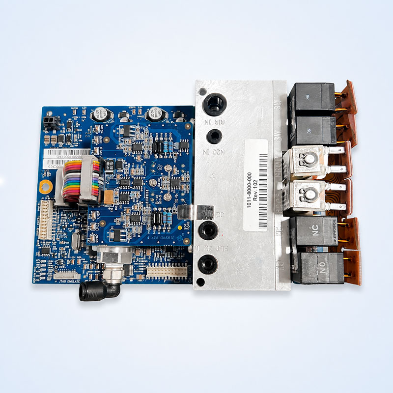
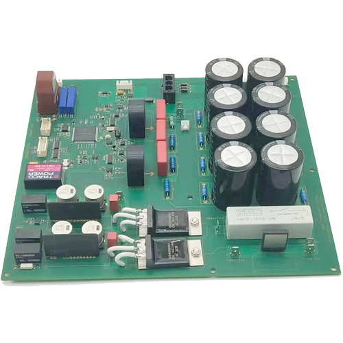
Industrial control power supply PCBA

Industrial Control

Lead-Free HASL, ENIG and selective hard gold for durable controls, connectors and power electronics.

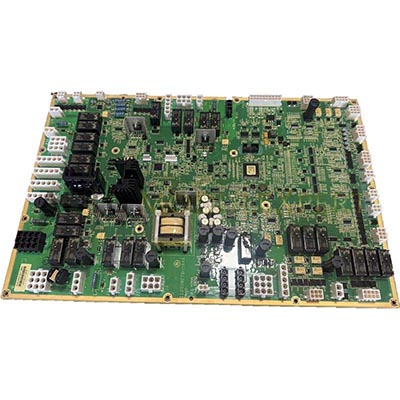
Automotive and EV charging control PCBA

Automotive Electronics

ENIG, ENEPIG and selective gold systems for dense assemblies, sensors and reliable contact areas.

Renewable energy PCB assembly

Renewable Energy

Lead-Free HASL, ENIG and selective contact finishes for inverters, BMS and energy-control hardware.

Medical device control PCB assembly

Medical Devices

ENIG, ENEPIG and application-specific gold for fine-pitch, cleanable and high-reliability electronics.

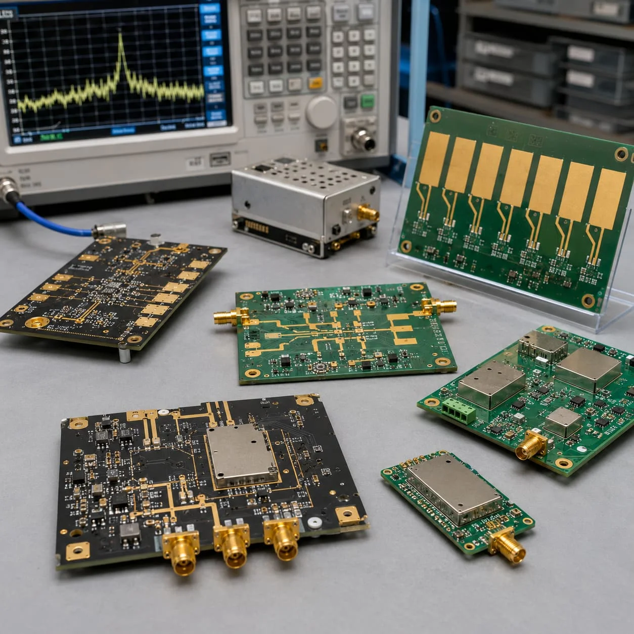
Telecommunications and RF PCB

Telecommunications

ENIG, immersion silver and reviewed EPIG options for RF modules, antenna systems and signal transmission.

Connected consumer electronics PCBA

Consumer Electronics

OSP, ENIG and Lead-Free HASL for compact, fine-pitch and cost-sensitive electronic products.

Frequently Asked Questions

PCB Surface Finish FAQs

What is the most common PCB surface finish?

Lead-Free HASL, ENIG and OSP are widely used. The best choice depends on component pitch, assembly requirements, operating environment and target cost.

Is ENIG suitable for BGA components?

Yes. ENIG provides a flat pad surface and is commonly selected for BGA, QFN and fine-pitch SMT components.

What is the difference between ENIG and Hard Gold?

ENIG is primarily selected for flat solderable pads. Hard Gold is electroplated for wear resistance and is commonly used on connector fingers and repeated-contact surfaces.

Which finish is best for gold fingers?

Electroplated Hard Gold is normally recommended because it provides the wear resistance required for repeated insertion and contact.

Which surface finishes are lead-free?

Lead-Free HASL, ENIG, OSP, Immersion Silver, Immersion Tin and ENEPIG can support lead-free PCB manufacturing.

What is nickel-free palladium gold (EPIG)?

EPIG is Electroless Palladium Immersion Gold without a nickel barrier. KKPCB supports Pd 1–5 µin and Au 1–5 µin (each approximately 0.025–0.127 µm) for reviewed applications.

Can two finishes be used on one PCB?

Yes. Selective combinations such as ENIG plus local Hard Gold can separate solderable pads from wear-resistant contacts when clearly defined on the fabrication drawing.

Can KKPCB recommend the correct finish?

Yes. Submit Gerber files, material and application requirements, finish thickness, full-board or selective areas, and compliance needs for engineering review.

Engineering Support

Need Help Selecting a PCB Surface Finish?

Send us your PCB files and application requirements. Our engineers will review the design and recommend a suitable finish for your assembly, reliability and cost targets.

Upload Gerber Files / Request a Quote