The Growing Demand for Advanced Electronic Film Materials
As modern electronics continue evolving toward:
- flexible electronics
- wearable devices
- transparent displays
- high-speed semiconductors
- advanced sensors
- next-generation communication systems
the demand for high-performance conductive and semiconductor films has increased dramatically.
Conventional thin-film materials often face major limitations involving:
- low mechanical flexibility
- brittle fracture behavior
- reduced carrier mobility
- thermal instability
- poor large-area manufacturability
In advanced electronic systems, achieving both:
- high ductility
- ultra-high carrier mobility
has traditionally been difficult because improving one property often degrades the other.
To overcome these challenges, researchers and manufacturers increasingly explore:
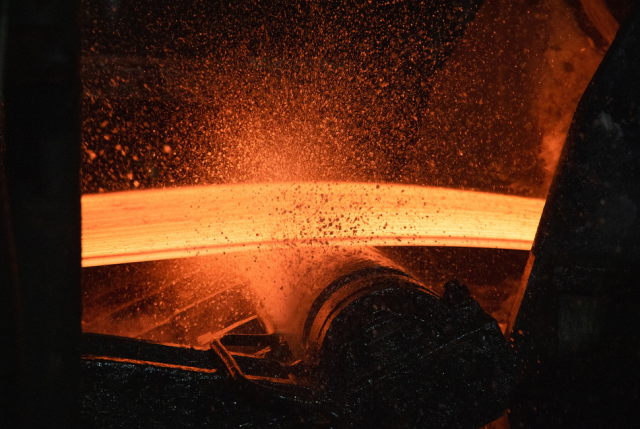
- warm-metallurgy processing technology
Warm-metallurgy processing enables the fabrication of advanced thin films with:
- improved crystal structure
- enhanced grain alignment
- reduced defect density
- superior mechanical flexibility
- exceptional electron mobility
This article explores:
- warm-metallurgy processing principles
- high-ductility thin-film technology
- ultra-high mobility electronic films
- advanced semiconductor film engineering
- flexible electronic materials
- manufacturing advantages
- future applications in advanced electronics
What Is Warm-Metallurgy Processing?
Definition of Warm-Metallurgy Processing
Warm-metallurgy processing refers to:
- controlled material processing performed at intermediate temperatures
typically between:
- room temperature
and: - full high-temperature metallurgical processing conditions.
This approach allows:
- optimized atomic diffusion
- controlled grain growth
- improved microstructure engineering
- enhanced mechanical properties
Warm-metallurgy techniques are increasingly used in:
- semiconductor film fabrication
- conductive thin-film processing
- flexible electronic materials
- advanced nanomaterials
Why Warm-Metallurgy Processing Is Important
Traditional high-temperature processing may cause:
- excessive grain coarsening
- thermal stress
- film cracking
- substrate damage
Low-temperature processing may lead to:
- poor crystallinity
- low carrier mobility
- structural defects
Warm-metallurgy processing creates a balance by enabling:
- controlled crystal formation
- defect reduction
- improved film flexibility
- enhanced electronic performance
Understanding High Ductility in Thin Films
What Is Ductility?
Ductility refers to:
- a material’s ability to deform without cracking or breaking.
For electronic thin films, high ductility enables:
- bending
- stretching
- folding
- repeated mechanical movement
without:
- electrical failure
- structural fracture
Why High Ductility Matters in Modern Electronics
High-ductility films are essential for:
- flexible displays
- wearable electronics
- foldable smartphones
- biomedical sensors
- flexible PCB systems
- soft robotics
Traditional brittle films may fail under:
- repeated mechanical stress
- bending cycles
- thermal expansion
Warm-metallurgy processing improves:
- grain boundary engineering
- dislocation movement
- stress distribution
resulting in:
- superior mechanical flexibility
- enhanced structural reliability
What Are Ultra-High Mobility Films?
Definition of Carrier Mobility
Carrier mobility describes:
- how easily electrons or holes move through a semiconductor material.
Higher carrier mobility enables:
- faster signal transmission
- lower power consumption
- improved switching speed
- higher-frequency operation
Ultra-high mobility films are critical for:
- advanced transistors
- RF electronics
- high-speed computing
- optoelectronic systems
How Warm-Metallurgy Processing Improves Carrier Mobility
Warm-metallurgy processing can reduce:
- grain boundary scattering
- crystal defects
- impurity concentration
- structural disorder
This improves:
- electron transport efficiency
- conductivity
- semiconductor performance
Enhanced crystallinity enables:
- ultra-high carrier mobility
- low electrical resistance
- stable electronic behavior
Key Mechanisms Behind Warm-Metallurgy Thin-Film Enhancement
1. Grain Structure Optimization
Controlled thermal processing improves:
- grain orientation
- grain size uniformity
- crystal continuity
Benefits:
- reduced defect density
- improved ductility
- enhanced conductivity
2. Reduced Internal Stress
Warm processing minimizes:
- residual stress
- thermal mismatch
- microcracking
This enhances:
- mechanical durability
- film stability
- flexible device reliability
3. Improved Atomic Diffusion
Moderate thermal energy supports:
- controlled atomic movement
- defect healing
- interface stabilization
Resulting in:
- higher crystal quality
- improved electronic properties
4. Enhanced Interface Engineering
Warm-metallurgy processing improves:
- film-to-substrate adhesion
- interface smoothness
- electrical continuity
This is critical for:
- multilayer semiconductor devices
- flexible electronics
- transparent conductive films
Types of Films Benefiting from Warm-Metallurgy Processing
1. Semiconductor Thin Films
Applications:
- thin-film transistors (TFTs)
- flexible processors
- advanced IC packaging
- oxide semiconductors
- silicon thin films
- compound semiconductors
2. Transparent Conductive Films
Used in:
- OLED displays
- touch panels
- flexible displays
- solar cells
Benefits:
- high transparency
- excellent conductivity
- mechanical flexibility
3. Metal Nanofilms
Applications:
- RF electronics
- flexible antennas
- wearable sensors
Warm-metallurgy processing improves:
- conductivity
- fatigue resistance
- flexibility
4. 2D Electronic Materials
Including:
- graphene
- transition metal dichalcogenides (TMDs)
Benefits:
- ultra-high mobility
- advanced flexible electronics capability
Applications of High-Ductility Ultra-High Mobility Films
1. Flexible Electronics
Applications:
- foldable smartphones
- flexible tablets
- wearable sensors
Benefits:
- repeated bending durability
- stable electrical performance
2. High-Speed Semiconductor Devices
Ultra-high mobility films improve:
- transistor switching speed
- RF signal processing
- AI computing efficiency
3. Flexible RF and Microwave Electronics
Applications:
- wearable communication devices
- flexible RF antennas
- smart textiles
4. Biomedical Electronics
Used in:
- skin-mounted sensors
- implantable electronics
- flexible health monitoring systems
5. Advanced Display Technology
Applications:
- OLED panels
- transparent displays
- rollable displays
6. Flexible Solar Cells
High-ductility films support:
- bendable photovoltaic systems
- lightweight renewable energy devices
Manufacturing Challenges in Warm-Metallurgy Film Processing
1. Precise Temperature Control
Processing temperatures must remain carefully optimized to avoid:
- excessive grain growth
- substrate damage
- thermal instability
2. Uniform Large-Area Processing
Maintaining consistent film quality across:
- large substrates
- flexible panels
remains technically challenging.
3. Material Compatibility
Different film materials may respond differently to:
- thermal diffusion
- mechanical stress
- interface reactions
4. High Manufacturing Cost
Advanced thin-film processing may require:
- specialized equipment
- precision thermal control
- advanced deposition systems
Future Trends in Warm-Metallurgy Thin-Film Technology
1. Ultra-Flexible Semiconductor Systems
Supporting:
- stretchable electronics
- soft robotics
- wearable AI devices
2. Next-Generation High-Mobility Materials
Including:
- graphene electronics
- 2D semiconductor integration
-
quantum materials
3. Advanced Flexible RF Electronics
Enabling:
- 6G communication
- wearable RF systems
- flexible mmWave devices
4. AI-Optimized Materials Engineering
Using:
- machine learning material discovery
- predictive microstructure simulation
- intelligent thermal optimization
Conclusion
Warm-metallurgy processing provides a powerful approach for developing advanced electronic films with:
- high ductility
- ultra-high carrier mobility
- excellent mechanical flexibility
- superior electronic performance
By optimizing:
- grain structure
- atomic diffusion
- defect reduction
- interface engineering
manufacturers can achieve:
- flexible high-speed electronics
- reliable wearable devices
- advanced semiconductor systems
- next-generation RF technologies
As electronics continue evolving toward:
- flexible integration
- lightweight systems
- high-speed communication
- intelligent wearable platforms
warm-metallurgy processing will become increasingly important for the future of:
- semiconductor engineering
- flexible electronics
- advanced thin-film technology
- ultra-high-performance electronic materials
