LoRa PCB Antenna Design: Tips, Engineering Principles, and Best Practices
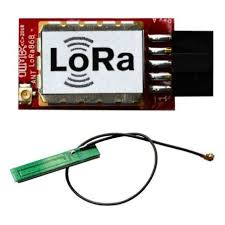
LoRa (Long Range) technology enables ultra-low-power, long-range wireless communication, making it a backbone protocol in IoT applications such as smart agriculture, smart meters, industrial monitoring, and asset tracking.
But no matter how advanced the LoRa transceiver is, its actual communication range is ultimately determined by the PCB antenna design.
Poor antenna design results in:
- Shorter transmission range
- Unstable RSSI/SNR
- Higher current consumption
- Failure to pass RF certification
This article provides a professional, step-by-step engineering guide to designing high-performance LoRa PCB antennas.
1. Fundamentals of LoRa PCB Antenna Design
1.1 Antenna Basics
An antenna converts electrical energy into electromagnetic waves. LoRa operates mainly at:
-
EU: 868 MHz
-
US: 915 MHz
-
Asia: 433 MHz (optional region)
At these frequencies, antenna length is determined by:
L = c / (4f)
Example:
Quarter-wave length at 915 MHz ≈ 82 mm
Quarter-wave length at 868 MHz ≈ 86.3 mm
Because the PCB cannot accommodate antennas this long, engineers use tuned, miniaturized versions such as IFA or meandered structures.
2. Key PCB Antenna Design Considerations
2.1 Frequency Accuracy
The antenna must resonate exactly at 868/915 MHz.
Even 2–3% deviation reduces gain significantly.
2.2 Ground Plane Requirements
The ground plane acts as the antenna’s “mirror.” Insufficient ground causes:
-
Reduced radiation efficiency
-
Poor impedance matching
-
Lower transmission distance
General rules:
-
Ensure ≥ wavelength/10 ground length
-
Keep ground continuous without gaps
2.3 Antenna Size
A quarter-wave structure is recommended, or a shortened IFA.
Rules of thumb:
-
Longer = wider bandwidth
-
Larger = higher radiation efficiency
2.4 Impedance Matching
The antenna must be matched to 50 Ω.
Without proper matching:
-
Signal reflects back into RF chain
-
PA (power amplifier) may overheat
-
RSSI and range degrade
2.5 Radiation Pattern Requirements
Depending on device orientation:
-
Omnidirectional: Sensors / trackers
-
Directional: Base stations, gateways
Pattern optimization is addressed later in the article.
3. LoRa PCB Antenna Design Techniques

Below are the three most common antenna structures in LoRa devices.
3.1 Monopole PCB Antenna
A classical and widely used antenna.
Structure
-
A quarter-wave radiating element
-
Ground plane acts as mirror
Advantages
✔ Simple
✔ Low cost
✔ Wide bandwidth
Disadvantages
✘ Requires relatively large PCB ground area
Use Cases
-
LoRa trackers
-
Smart metering
-
Outdoor sensors
3.2 Patch Antenna
A microstrip patch over a ground plane.
Advantages
✔ Highly directional
✔ Higher gain
✔ Great for long-range connections
Disadvantages
✘ Larger size
✘ Needs precise tuning
Use Cases
-
Gateways
-
Smart city nodes
-
Fixed installations
3.3 Inverted-F Antenna (IFA) / Meandered IFA
The most popular PCB antenna for compact LoRa devices.
Advantages
- Compact size
- Tunable
- Stable performance
- Easy to match
Disadvantages
- Requires careful PCB layout
- Sensitive to enclosure materials
Use Cases
-
Wearable LoRa devices
-
Battery-operated IoT sensors
-
Handheld terminals
4. Advanced LoRa Antenna Engineering Techniques
4.1 Impedance Matching Techniques
A matching network typically consists of:
-
Series inductor + parallel capacitor (π-network)
-
Shunt L/C
-
Balun transformer (if differential path exists)
Matching goals:
-
Achieve 50 Ω impedance
-
Minimize return loss (< –10 dB preferred)
-
Maximize radiated power
Tools used:
-
VNA (Vector Network Analyzer)
-
Smith chart
-
RF simulation (HFSS / CST / ADS)
4.2 Antenna Tuning Strategies
Antenna tuning adjusts resonance frequency.
Method 1: VNA + S11 Parameter Measurement
-
Ideal S11 < –15 dB at target band
-
Adjust antenna length or matching components
Method 2: Length Trimming
Lengthening → shifts lower frequency
Shortening → shifts higher frequency
Method 3: Capacitive Loading
Add capacitor to lower resonance frequency without increasing physical size.
4.3 Radiation Pattern Optimization
Goal: Maximize radiation in the directions important to the device.
Optimization strategies
-
Increase ground size
-
Add keep-out zone around antenna
-
Avoid metal enclosures
-
Avoid routing underneath antenna
-
Use simulation tools to detect nulls and distortions
Testing Tools
-
Anechoic chamber
-
3D near-field scanner
-
Far-field range tests
5. PCB Layout Best Practices for LoRa Antennas
Keep antenna area free of copper
Ensure isolation from high-speed traces
Place antenna at edge of PCB
Use a continuous ground plane
Avoid battery or metal shielding near antenna
Add tuning pads for π-network
Maintain 50 Ω feedline with controlled impedance
A bad layout can reduce the range from 10 km → 500 m.
6. Final Recommendations
To achieve optimal LoRa antenna performance:
- Use a 50-ohm controlled impedance feedline
- Simulate before fabricating
- Always include a matching network
- Test in final enclosure
Perform over-the-air range tests
When done properly, LoRa PCB antennas can easily reach:
-
2–5 km suburban range
-
10–15 km rural / line-of-sight
-
>1 km dense urban environment
Conclusion
LoRa PCB antenna design is both an art and a science. It requires understanding RF principles, antenna structures, PCB layout impacts, enclosure effects, and advanced matching/tuning techniques.
By following the engineering methods outlined above, you can create LoRa devices with:
- Long transmission distance
- Stable performance
- Low power consumption
- High RF efficiency
- Certification-ready antenna behavior
Whether you are designing LoRa sensors, smart meters, gateways, or tracking devices, a properly designed PCB antenna is the key to unlocking LoRa’s full communication potential.
