//Smart home electronics manufacturing services provideSmart Home PCB Assembly service
Smart homes provide intelligent insights into energy usage, helping homeowners become more energy-efficient, reduce costs, and minimize environmental impact. By identifying areas of unnecessary energy consumption, smart home systems enable targeted energy savings while offering real-time monitoring and remote control of home devices, creating a more convenient, safe, and sustainable living environment.
Smart Home PCB Assembly is a critical component in this ecosystem, enabling the functionality, connectivity, and automation of smart home devices and systems. These PCBs serve as the backbone for components such as sensors, microcontrollers, actuators, and communication modules, providing a reliable platform for electrical power distribution and seamless interconnection. Designed for high reliability, durability, and low power consumption, smart home PCBs ensure that devices perform consistently, even in battery-powered or energy-sensitive applications.
At KKPCB, we specialize in delivering customized PCB solutions for smart home applications, including PCB design, prototyping, assembly, and full-scale production. Our PCBs are built using premium materials and advanced manufacturing processes, adhering to strict quality standards to guarantee long-term reliability and stable performance. With fast delivery, professional technical support, and turnkey services, KKPCB helps customers bring innovative smart home products to market efficiently and confidently, ensuring every device meets the highest standards of performance and safety.
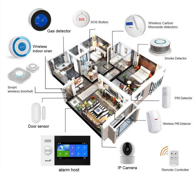
// Smart Home PCB AssemblySmart Home PCB Applications
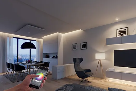
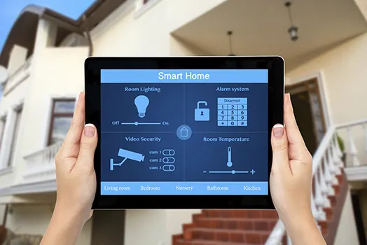
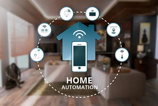
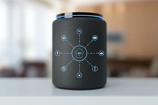
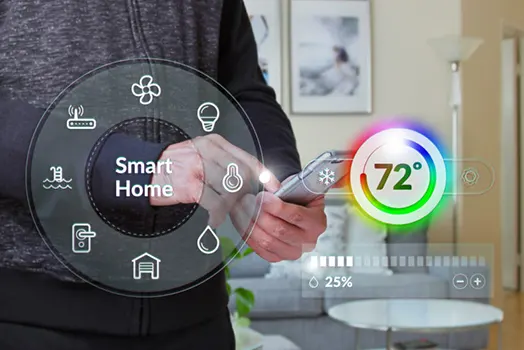
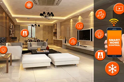
// Types of Smart Home PCB AssemblyHere are some key aspects of PCB assembly for smart home applications
Smart home PCB assemblies are essential for enabling the functionality, connectivity, and automation of modern connected homes. Key aspects include:
-
Home Automation: These PCBs integrate sensors, microcontrollers, wireless communication modules, and other components to enable control and monitoring of lighting, security systems, door locks, appliances, and other connected devices.
-
Connectivity: Smart home PCBs incorporate wireless technologies such as Wi-Fi, Bluetooth, and cellular modules to facilitate seamless communication between devices, mobile applications, and central control hubs.
-
Sensor Integration: They support various sensors—temperature, humidity, occupancy, motion, light, and more—capturing and processing environmental data to enable automation and intelligent control.
-
User Interfaces: PCB assemblies include touchscreens, buttons, keypads, or voice control modules to allow users to manage and adjust smart home devices and automation routines easily.
-
Power Management: Efficient power management circuits, such as voltage regulators, power switches, and battery chargers, ensure reliable operation and optimized energy consumption.
-
Security and Privacy: These PCBs integrate encryption modules, secure authentication chips, tamper detection circuits, and secure communication protocols to protect user data and maintain network integrity.
-
Integration with Home Infrastructure: Smart home PCBs are designed for compatibility with standard home electrical wiring and appliances, ensuring seamless integration with existing infrastructure while maintaining optimal form factor and performance.
At KKPCB, we design and manufacture custom smart home PCB assemblies that meet the highest standards of reliability, performance, and energy efficiency, helping you bring innovative smart home products to market quickly and confidently.

Types of Smart Home PCB Assembly
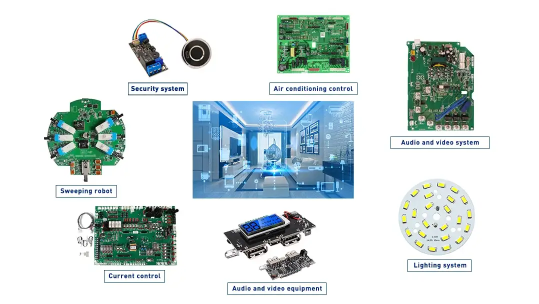
- Lighting Control PCBA: These PCBAs are designed for automating and controlling lighting systems within a smart home. They integrate communication modules, microcontrollers, and power management circuits to enable remote control, scheduling, dimming, color changing, and other lighting functionalities.
- Thermostat Control PCBA: Thermostat control PCBAs are used in smart home heating, ventilation, and air conditioning (HVAC) systems. These PCBAs incorporate temperature sensors, communication modules, and control circuits to regulate and automate temperature settings based on user preferences, schedules, or environmental conditions.
- Security System PCBA: Security system PCBAs are the backbone of smart home security solutions. They integrate components such as sensors (motion sensors, door/window sensors), control circuits, communication modules, and alarm triggering circuits. These PCBAs enable intrusion detection, video surveillance, access control, and remote monitoring functionalities.
- Home Automation Hub PCBA: Home automation hub PCBAs act as central control units for smart home systems. They integrate microcontrollers, communication modules (Wi-Fi, Zigbee, Z-Wave, etc.), and user interface components. These PCBAs facilitate the integration, management, and control of multiple smart devices within a smart home ecosystem.
- Voice Assistant PCBA: Voice assistant PCBAs incorporate voice recognition and processing technologies, enabling voice-controlled interactions with smart home devices. These PCBAs integrate microphones, audio processing circuits, communication modules, and AI algorithms to interpret voice commands and control various smart home functions.
- Appliance Control PCBA: These PCBAs are used to control and monitor smart appliances within a smart home. They integrate microcontrollers, communication modules, and power management circuits to enable remote control, energy monitoring, scheduling, and status feedback for appliances like refrigerators, ovens, washing machines, and more.
- Environmental Monitoring PCBA: Environmental monitoring PCBAs incorporate sensors for measuring environmental parameters such as temperature, humidity, air quality, or carbon dioxide levels within a smart home. These PCBAs provide data for automation, energy optimization, and user comfort purposes.
- Motor Control PCBA: Motor control PCBAs are used in smart home applications involving motorized devices such as motorized shades, curtains, or garage doors. These PCBAs integrate motor control circuits, sensors, and communication modules to enable remote control, automation, and position monitoring of motorized systems.
// FREQUENTLY ASKED QUESTIONS (FAQ)Smart Home PCB Frequent Questions
Smart home PCBs can be used in a variety of applications such as smart lighting, thermostats, security systems, appliances, speakers, entertainment systems, HVAC systems, irrigation systems, smart plugs, and sensors. They enable remote control, automation, and integration of devices to improve convenience, safety, and energy efficiency in the home. These PCBs are essential for the seamless operation and connectivity of a smart home environment.
Smart Home PCB quality assurance requirements include adhering to industry standards, using high-quality materials and components, and conducting thorough design verification. Controlled manufacturing processes and extensive testing, such as automated optical inspection (AOI), functional, environmental, electrical, and reliability tests, are essential. Proper documentation and traceability ensure accountability and continuous improvement, guaranteeing reliable and high-performance PCBs for smart home devices.
Smart home PCB design must consider connectivity, power management, compactness, component integration, thermal management, signal integrity, durability, environmental resistance, security, compliance with industry standards, ease of manufacture, and scalability. Addressing these factors ensures the creation of reliable, efficient, and secure smart home devices that meet consumer expectations and regulatory requirements.
Smart home PCB assembly types include Surface-Mount Technology (SMT) for high-density designs, Through-Hole Technology (THT) for robust connections, and Mixed Technology for combining both methods. Flexible PCB Assembly suits designs requiring flexibility, while Rigid-Flex PCB Assembly integrates both rigid and flexible sections. Hybrid PCB Assembly combines traditional and advanced technologies. Each type is selected based on the specific design needs, component density, flexibility, and durability requirements of smart home devices.
Smart home PCB products are crucial because they form the backbone of modern home automation systems. They enable connectivity, control, and integration of various smart devices, such as thermostats, lighting systems, security cameras, and appliances. By facilitating wireless communication and efficient power management, smart home PCBs enhance convenience, energy efficiency, and security in everyday life. Their compact design and reliability ensure that smart home devices perform optimally, contributing to a seamless and user-friendly smart home experience.
For smart home PCB assembly, essential files include Gerber files for layout details, Bill of Materials (BOM) for component specifications, Pick and Place files for component placement, and schematic diagrams for circuit design. Additionally, Assembly Drawings guide component placement and soldering, Stencil Files ensure precise solder paste application, Test Specifications outline testing procedures, and Design for Assembly (DFA) Guidelines optimize the assembly process. These files collectively ensure accurate manufacturing, assembly, and testing of smart home PCBs.

